Crosstalk in a high-speed PCB occurs when energy from one signal trace unintentionally couples into another nearby trace, causing noise, timing errors, EMI problems, and possible data corruption. It is mainly caused by excessive parallel routing, insufficient trace spacing, poor return path design, improper stackup, uncontrolled impedance, and weak differential pair routing practices.
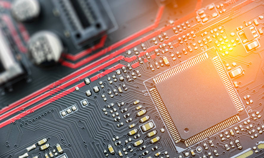
In high-speed PCB design, crosstalk is not only a layout issue. It is also related to stackup planning, material selection, impedance control, via transitions, reference planes, and manufacturing consistency. A design may look correct in schematic form, but if signal traces are routed too close together or lose their reference plane, the final board may suffer from signal integrity problems.
For companies developing communication equipment, industrial controllers, automotive electronics, medical devices, or high-speed computing hardware, crosstalk can lead to unstable performance, failed compliance testing, delayed product launches, and repeated PCB revisions. That is why working with an experienced high-speed PCB manufacturing partner is important when the board involves fast edge rates, dense routing, controlled impedance, or differential pairs.
Industry design resources commonly emphasize the importance of solid reference planes, sufficient spacing, controlled impedance, and careful return path management for high-speed PCB signal integrity.
What Is Crosstalk in High-Speed PCB Design?
PCB crosstalk is unwanted electromagnetic coupling between two or more signal traces. The trace that generates the interference is often called the aggressor, while the trace affected by the noise is called the victim.
In low-speed circuits, small amounts of coupling may not cause visible problems. In high-speed PCB applications, however, the same coupling can become critical because fast signal edges contain high-frequency energy. Even when the clock frequency is not extremely high, a fast rise time or fall time can make the interconnect behave like a transmission line.
A PCB should be treated as “high-speed” when signal rise time, trace length, and impedance behavior begin to affect waveform quality, not only when the clock frequency looks high.
Crosstalk can appear as:
| Crosstalk Symptom | Possible Result in High-Speed PCB |
|---|---|
| Noise spikes on quiet lines | False switching or logic errors |
| Eye diagram closure | Reduced timing margin |
| Jitter increase | Unstable data transmission |
| EMI increase | Compliance test failure |
| Signal reflection combined with coupling | Difficult debugging after assembly |
| Intermittent communication failure | Product reliability issues |
For B2B buyers, the key point is simple: if your product relies on USB, Ethernet, PCIe, DDR, LVDS, SerDes, RF control lines, or high-speed sensor interfaces, crosstalk should be considered early in the PCB design and manufacturing stage.
Why Crosstalk Matters for High-Speed PCB Customers
Crosstalk is not just a theoretical signal integrity topic. It can directly affect product cost, delivery time, and field reliability.
When crosstalk is not properly controlled, companies may face:
- Failed prototype validation
- Repeated PCB layout revisions
- Higher debugging cost
- Signal integrity simulation delays
- EMI/EMC certification failure
- Reduced product stability in real operating environments
- Difficulty scaling from prototype to mass production
For example, a prototype may pass basic power-on testing but fail under full data load, high temperature, or long cable operation. In many cases, the root cause is not the IC itself but the interconnect environment: trace spacing, return path discontinuity, via stub, poor layer transition, or incorrect impedance.
In B2B high-speed PCB projects, preventing crosstalk before fabrication is usually more cost-effective than debugging it after assembly.
This is why PCB manufacturers serving high-speed applications must understand not only fabrication tolerances, but also impedance control, stackup communication, material behavior, and engineering review.
Main Causes of Crosstalk in High-Speed PCB
1. Long Parallel Trace Routing
Long parallel routing is one of the most common causes of PCB crosstalk. When two high-speed traces run side by side for a long distance, the electromagnetic field from one trace can couple into the adjacent trace.
The longer the parallel run, the stronger the potential coupling. This is especially risky for clock lines, reset lines, data buses, and sensitive analog or RF-adjacent signals.
A commonly used layout rule is to increase trace spacing when signals must run in parallel. Some design guidelines refer to conservative spacing rules such as 3W, where spacing is related to trace width, but the correct value still depends on edge rate, layer structure, dielectric height, impedance target, and acceptable noise budget.
2. Insufficient Trace Spacing
Trace spacing directly affects capacitive and inductive coupling. When traces are close together, electric and magnetic field interaction becomes stronger.
In dense high-speed boards, engineers often try to save space by routing traces close to each other. However, aggressive routing density can increase crosstalk risk, especially if the design does not include proper simulation, stackup planning, and design rule constraints.
| Trace Spacing Condition | Crosstalk Risk | Engineering Comment |
|---|---|---|
| Very tight spacing between fast signals | High | Requires simulation and strict constraints |
| Moderate spacing with solid reference plane | Medium | Often acceptable if impedance is controlled |
| Wider spacing for clocks and critical nets | Lower | Preferred for sensitive high-speed lines |
| Random spacing without rules | Unpredictable | Risky for production repeatability |
3. Poor Return Path Design
High-speed signals do not travel only through the visible copper trace. They also depend on a return current path, usually through an adjacent reference plane. If the return path is broken by a plane split, void, poor via transition, or incorrect layer change, the return current must detour.
That detour increases loop area and can create stronger electromagnetic radiation and coupling into nearby nets. High-speed return currents typically follow the path of lowest impedance, often directly beneath the signal trace when a continuous reference plane is available.
A continuous reference plane under high-speed traces is one of the most practical ways to reduce crosstalk, EMI, and signal distortion.
4. Improper PCB Stackup
PCB stackup has a major influence on crosstalk. If a high-speed signal layer is far from its reference plane, the electromagnetic field spreads more widely. This can increase coupling to nearby traces.
A well-designed stackup keeps high-speed signal layers close to solid ground or power reference planes. It also separates noisy power sections from sensitive high-speed routes and supports controlled impedance.
For many high-speed PCB projects, stackup discussion should happen before final layout, not after routing is complete.
5. Uncontrolled Impedance
Impedance discontinuity can worsen signal integrity problems. Although impedance mismatch is not the same as crosstalk, reflections and crosstalk often appear together in high-speed PCB debugging.
If trace width, dielectric thickness, copper thickness, or material properties are not controlled, the board may deviate from the intended impedance. This can cause waveform distortion, eye diagram degradation, and timing uncertainty.
Controlled impedance is especially important for interfaces such as USB, Ethernet, PCIe, HDMI, LVDS, MIPI, and DDR.
6. Poor Differential Pair Routing
Differential pairs are designed to carry equal and opposite signals. When routed correctly, they help reject common-mode noise and support reliable high-speed transmission. However, differential pairs can still suffer from crosstalk if the pair is unbalanced, routed too close to other pairs, or affected by inconsistent spacing.
Key problems include:
- Unequal trace length
- Inconsistent pair spacing
- Pair routed over plane splits
- Excessive skew
- Nearby aggressor signals
- Too many layer transitions
- Incorrect via design
Some design resources refer to spacing rules between differential pairs, but spacing should always be validated according to the actual interface, stackup, and design constraints.
Types of Crosstalk: Capacitive, Inductive, Near-End, and Far-End
Understanding crosstalk types helps engineers decide how to prevent them.
Capacitive Coupling
Capacitive coupling occurs through the electric field between adjacent conductors. When voltage changes quickly on the aggressor trace, part of that energy couples into the victim trace.
It becomes more serious when:
- Traces are close together
- Parallel routing length is long
- Signal edges are fast
- Reference plane is far away
- Victim line has high impedance
Inductive Coupling
Inductive coupling occurs through magnetic field interaction. When current changes rapidly on one trace, it can induce voltage in a nearby trace.
It becomes more serious when:
- Return current path is poor
- Loop area is large
- Adjacent traces run in parallel
- Ground reference is discontinuous
- High-current switching signals are close to sensitive signals
Near-End Crosstalk and Far-End Crosstalk
| Crosstalk Type | Where It Appears | Common Concern |
|---|---|---|
| Near-End Crosstalk, NEXT | At the same end as the aggressor source | Can create noise at receivers near the driver side |
| Far-End Crosstalk, FEXT | At the far end of the victim line | Can affect timing and data eye quality |
| Common-mode crosstalk | Appears as shared-mode noise | Can increase EMI radiation |
| Differential crosstalk | Between differential pairs | Can degrade high-speed serial links |
NEXT and FEXT behavior depends on trace geometry, dielectric properties, routing layer, coupling length, and termination. For critical interfaces, simulation or signal integrity review is strongly recommended.
Key Factors That Increase Crosstalk Risk
| Factor | Why It Matters | Prevention Method |
|---|---|---|
| Fast rise/fall time | More high-frequency energy | Apply high-speed routing rules even if clock is moderate |
| Long parallel traces | More coupling length | Reduce parallelism or increase spacing |
| Tight routing density | Stronger field interaction | Define spacing constraints by net class |
| Broken reference plane | Return current detour | Keep solid reference planes under signals |
| Poor layer transition | Return path discontinuity | Add nearby ground return vias |
| Uncontrolled impedance | More reflections and waveform distortion | Use controlled impedance stackup |
| Inconsistent differential pair routing | Skew and mode conversion | Maintain pair symmetry and spacing |
| No simulation review | Risks found too late | Simulate critical nets before fabrication |
Cadence design guidance also emphasizes routing high-speed transmission lines with adjacent reference planes and using return path vias when layer changes are necessary.
How to Prevent Crosstalk in High-Speed PCB Layout
1. Increase Spacing Between Critical Traces
Increasing spacing is one of the most direct ways to reduce crosstalk. However, spacing should not be applied randomly. Engineers should classify nets according to signal type and risk level.
For example:
| Net Type | Suggested Routing Priority |
|---|---|
| Clock signals | Keep away from sensitive and parallel high-speed nets |
| High-speed differential pairs | Route with controlled spacing and length matching |
| Reset/control lines | Avoid routing beside noisy clocks |
| Analog/sensor lines | Separate from high-speed digital routes |
| Power switching nodes | Keep away from high-speed and low-level signals |
The spacing required to prevent crosstalk depends on edge rate, trace geometry, dielectric height, stackup, and acceptable noise margin—not only on trace width.
2. Reduce Long Parallel Runs
Avoid routing high-speed signals side by side for long distances. If two traces must cross, crossing at 90 degrees on adjacent layers may reduce broadside coupling compared with long parallel overlap.
Practical layout methods include:
- Use shorter routing paths
- Change routing direction between layers
- Separate aggressor and victim nets
- Avoid routing clocks near data lines for long distances
- Use net class rules in PCB design software
3. Use Solid Reference Planes
A solid ground plane under high-speed traces helps confine electromagnetic fields and provides a stable return path. This reduces loop area, EMI, and coupling.
Avoid:
- Routing high-speed traces across split planes
- Placing voids under critical signals
- Changing layers without nearby return vias
- Using fragmented copper reference areas for critical nets
When working with a controlled impedance PCB supplier, provide stackup requirements, impedance targets, copper thickness, material preferences, and critical net information early.
4. Optimize PCB Stackup Before Routing
Stackup should be planned before routing high-speed signals. A good stackup can reduce crosstalk and improve impedance control.
Common stackup goals include:
- Place high-speed signal layers adjacent to ground planes
- Use symmetrical layer construction when possible
- Control dielectric thickness for impedance stability
- Separate noisy power layers from sensitive signals
- Keep return paths continuous
5. Apply Controlled Impedance Design
Controlled impedance helps maintain predictable signal behavior. For high-speed PCB manufacturing, impedance depends on trace width, spacing, copper thickness, solder mask, dielectric constant, dielectric height, and fabrication tolerance.
A reliable PCB manufacturer should be able to support:
- Single-ended impedance control
- Differential impedance control
- Stackup review
- Impedance coupon testing when required
- Material selection guidance
- Production tolerance communication
6. Route Differential Pairs Correctly
Differential pairs should be routed with consistent spacing and length matching. The pair should remain symmetrical and should avoid unnecessary stubs, vias, and discontinuities.
Good differential pair practices include:
- Maintain consistent intra-pair spacing
- Match lengths according to interface requirements
- Avoid routing over plane splits
- Keep pairs away from unrelated aggressor signals
- Use proper via transitions
- Avoid unnecessary neck-down sections
7. Use Ground Vias and Guard Traces Carefully
Guard traces can help in some layouts, but they must be used correctly. A guard trace without frequent ground stitching may not be effective and can even create unexpected behavior.
Ground stitching vias can help provide a return path and reduce coupling, especially around sensitive or high-speed regions. However, they should be planned based on stackup, signal type, and available board space.
8. Avoid Via Stubs and Poor Layer Transitions
Via stubs can create signal integrity issues at high frequencies. In very high-speed designs, back drilling, blind vias, buried vias, or optimized via structures may be considered.
Layer transitions should include nearby return vias so that the return current can move smoothly between reference planes.
9. Verify Critical Nets Before Fabrication
For high-speed PCB projects, design review should include more than DRC clearance checks.
Recommended checks include:
| Check Item | Purpose |
|---|---|
| Impedance calculation | Confirm trace geometry and stackup |
| Coupling review | Identify risky parallel routing |
| Return path inspection | Find plane splits and voids |
| Differential pair review | Confirm spacing, skew, and symmetry |
| Via transition review | Reduce discontinuities |
| SI simulation | Validate critical interfaces before production |
| Fabrication capability review | Match design rules with manufacturing limits |
Many modern PCB tools include crosstalk or signal integrity analysis functions that allow designers to identify coupling risks before fabrication.
Common Mistakes That Make PCB Crosstalk Worse
Mistake 1: Only Looking at Clock Frequency
A 100 MHz signal with very fast rise time may create more signal integrity concern than expected. Edge rate matters.
Mistake 2: Using Generic Spacing Rules Without Stackup Review
Rules such as 3W or 3H can be useful starting points, but they are not universal. Dense high-speed boards need stackup-specific constraints.
Mistake 3: Routing Over Split Planes
This is a common cause of return path discontinuity. A high-speed trace should not lose its reference plane.
Mistake 4: Treating Differential Pairs as Automatically Immune
Differential signaling is robust, but not magic. Poor symmetry, skew, and nearby aggressor signals can still cause problems.
Mistake 5: Choosing a PCB Supplier Only by Unit Price
For high-speed boards, the lowest unit price may not be the lowest project cost if impedance tolerance, material control, or engineering communication is weak.
Engineering and Purchasing Advice for High-Speed PCB Projects
If you are sourcing high-speed PCB fabrication, do not only send Gerber files and wait for quotation. Provide complete technical information so the supplier can evaluate manufacturability and impedance requirements.
Recommended information includes:
| Information to Provide | Why It Helps |
|---|---|
| Layer count and stackup target | Supports impedance and return path review |
| Controlled impedance values | Helps define trace width and spacing |
| Critical net list | Allows engineering review of sensitive signals |
| Material requirement | Affects dielectric constant and loss |
| Copper thickness | Influences impedance and manufacturing tolerance |
| Surface finish | Important for assembly and long-term reliability |
| Testing requirement | Supports quality verification |
| Production volume | Helps optimize cost and process planning |
A capable high-speed PCB fabrication service should be able to discuss stackup, impedance, trace spacing, material selection, and process tolerance before production begins.
How to Choose a High-Speed PCB Supplier for Crosstalk-Sensitive Designs
When a PCB project involves crosstalk-sensitive routing, supplier capability matters. Here are practical criteria to evaluate.
1. Controlled Impedance Capability
Ask whether the supplier can manufacture single-ended and differential impedance boards with documented stackup and testing support.
2. Engineering Review Support
A good supplier should review stackup, impedance, manufacturability, and potential production risks before fabrication.
3. Material Knowledge
High-speed PCB materials affect loss, impedance, dielectric stability, and signal performance. The supplier should understand material options for your application.
4. Layer Registration and Process Control
Crosstalk and impedance are influenced by trace geometry and dielectric thickness. Manufacturing consistency is important for repeatable performance.
5. Prototype-to-Production Support
Your PCB supplier should support both engineering prototypes and stable production, especially if your project will move from validation to volume manufacturing.
For high-speed electronic products, working with a supplier experienced in high-speed PCB manufacturing can reduce communication gaps between design intent and fabrication reality.
FAQ
1. What causes crosstalk in high-speed PCB design?
Crosstalk in high-speed PCB design is mainly caused by electromagnetic coupling between nearby traces. Long parallel routing, tight trace spacing, poor return paths, improper stackup, and uncontrolled impedance can all increase coupling.
2. How do you reduce crosstalk in PCB layout?
To reduce crosstalk in PCB layout, increase spacing between critical traces, reduce long parallel runs, use solid reference planes, maintain controlled impedance, route differential pairs correctly, and verify high-speed nets before fabrication.
3. What is the best PCB trace spacing for crosstalk reduction?
There is no single best spacing for every PCB. Common rules such as 3W or 3H are useful starting points, but the proper spacing depends on edge rate, dielectric height, trace width, impedance target, stackup, and acceptable noise margin.
4. Can differential pairs have crosstalk?
Yes. Differential pairs can still experience crosstalk if they are routed too close to other pairs, have inconsistent spacing, cross plane splits, include excessive vias, or suffer from skew and imbalance.
5. Why is return path important in high-speed PCB crosstalk control?
The return path controls where high-speed current flows back to the source. If the return path is broken or forced to detour, loop area increases, which can increase EMI and coupling into nearby signals.
6. Does controlled impedance help prevent PCB crosstalk?
Controlled impedance does not eliminate crosstalk by itself, but it helps maintain predictable signal behavior. When combined with proper spacing, stackup, and return path design, it supports better signal integrity.
7. When should I choose a high-speed PCB manufacturer?
You should choose a high-speed PCB manufacturer when your board includes controlled impedance, differential pairs, fast digital interfaces, RF-sensitive circuits, dense multilayer routing, or strict signal integrity requirements.
Conclusion
Crosstalk in high-speed PCB design is caused by unwanted electromagnetic coupling between signal traces. It becomes more serious when traces are close together, routed in long parallel paths, poorly referenced to ground planes, or manufactured without controlled impedance.
The most effective prevention strategy is to combine good layout practice with proper PCB stackup, controlled impedance, return path continuity, differential pair discipline, and early engineering review.
For B2B projects, the PCB supplier should not only fabricate the board but also understand the manufacturing factors that affect signal integrity. If your design involves high-speed interfaces, dense routing, or crosstalk-sensitive signals, consider working with an experienced high-speed PCB manufacturer that can support stackup review, impedance control, and reliable production quality.