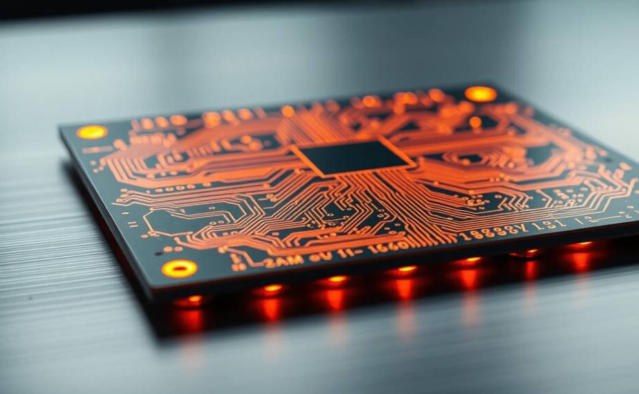
High-speed PCB in AI and GPU systems must support very fast data transmission, high current delivery, dense component placement, controlled impedance, thermal stability, and low-loss signal routing. Unlike standard PCBs, AI and GPU boards often need advanced stackups, high-speed differential pairs, strict power integrity control, and materials that can maintain stable electrical performance at high frequencies.
AI servers, GPU accelerator cards, edge AI devices, machine vision systems, and high-performance computing platforms all depend on reliable PCB design and manufacturing. When signals such as PCIe, GDDR, Ethernet, SerDes, and high-speed clock lines move across a PCB, the board becomes part of the signal path. Poor PCB design or unstable fabrication can cause signal loss, timing errors, EMI problems, excessive heat, or product instability.
For companies developing AI hardware or GPU-based systems, choosing the right high-speed PCB manufacturer is not only a purchasing decision. It is an engineering decision that affects prototype success, system reliability, certification risk, and production consistency.
Why AI and GPU Systems Need High-Speed PCB Design
AI and GPU systems process large volumes of data between processors, GPUs, memory devices, network interfaces, storage modules, and power management circuits. This creates three major PCB challenges:
- High-speed signal transmission
- High-current power delivery
- High-density thermal management
Modern AI hardware often uses PCIe, high-speed memory interfaces, multi-lane SerDes, Ethernet, clock distribution networks, and power rails with fast transient response. PCIe 6.0, for example, supports 64.0 GT/s raw data rate and uses PAM4 signaling, while PCIe 7.0 targets 128 GT/s and is aimed at data-intensive markets including AI/ML, HPC, cloud, and 800G Ethernet.
These interface speeds make PCB layout and manufacturing more sensitive than traditional digital boards. At high frequencies, even small variations in trace width, dielectric thickness, copper roughness, via design, and connector transitions can affect signal quality.
In AI and GPU hardware, the PCB is not just a carrier board; it is a controlled electrical interconnect system.
Core Applications of High-Speed PCB in AI and GPU Systems
High-speed PCBs are widely used across different AI and GPU hardware platforms.
| Application | Typical PCB Requirements | Key Design Focus |
|---|---|---|
| GPU accelerator cards | PCIe, memory routing, high-current power rails | Signal integrity, thermal reliability, impedance control |
| AI inference modules | Compact layout, high-speed I/O, edge computing interfaces | Miniaturization, EMI control, power efficiency |
| AI training servers | Multi-GPU interconnects, high-layer-count boards | Stackup control, low-loss materials, power distribution |
| Machine vision systems | Camera interfaces, FPGA/GPU processing | High-speed data capture, noise control |
| Data center networking | 100G/400G/800G interfaces, optical modules | SerDes routing, low insertion loss, crosstalk reduction |
| Embedded AI boards | CPU/GPU/NPU integration, memory interfaces | HDI design, thermal vias, manufacturability |
Different products may use different architectures, but they share one requirement: the PCB must preserve signal quality while supporting dense, high-power electronics.
Key Interfaces on AI and GPU PCBs
PCIe Interfaces
PCIe is one of the most important interfaces in GPU systems. It connects GPUs, CPUs, accelerators, storage devices, and expansion cards. As PCIe speeds increase, the PCB channel becomes more difficult to design.
A PCIe channel may include:
- PCB traces
- Vias
- Connectors
- Packages
- Retimers or redrivers
- Cables or backplanes
- Reference planes
For PCIe 5.0 and beyond, designers need to pay close attention to insertion loss, return loss, via stubs, impedance discontinuities, skew, and crosstalk. In many cases, PCIe routing requires simulation before manufacturing.
GPU Memory Interfaces
GPU boards may use GDDR, HBM-related interposers, or other memory architectures depending on the product type. GDDR7, for example, introduces PAM3 signaling and other improvements for high-frequency graphics memory operation. Industry sources report that GDDR7 data rates start at 32 Gbps per pin, with roadmaps toward higher bandwidth.
For PCB designers, high-speed memory routing requires tight length matching, controlled impedance, proper reference planes, stable power delivery, and careful breakout from dense packages.
SerDes and High-Speed Ethernet
AI servers and GPU clusters often require high-bandwidth networking. SerDes links, Ethernet interfaces, optical module connections, and switch ASICs place heavy demands on PCB materials and routing quality.
At these speeds, the board must be designed as a channel. The routing path, connector, via transition, material loss, and copper roughness all affect link performance.
NVLink and GPU-to-GPU Interconnects
Some AI systems use specialized GPU-to-GPU interconnects. NVIDIA states that its Blackwell architecture includes fifth-generation NVLink technology, and its NVLink Switch chip supports clusters beyond a single server with 1.8 TB/s interconnect capability.
Not every custom PCB project uses NVLink directly, but the broader trend is clear: AI hardware is moving toward higher bandwidth, lower latency, and more complex interconnect structures. This increases the importance of advanced high-speed PCB design.
Major PCB Design Challenges in AI and GPU Hardware
1. Signal Integrity
Signal integrity is the foundation of high-speed PCB performance. Problems such as reflection, attenuation, crosstalk, jitter, and impedance mismatch can cause unstable data transmission.
Common signal integrity risks include:
| Risk | Cause | Possible Impact |
|---|---|---|
| Reflection | Impedance discontinuity | Ringing, eye diagram closure |
| Insertion loss | Long trace, lossy material, rough copper | Weak signal at receiver |
| Crosstalk | Tight spacing between high-speed pairs | Noise coupling, data errors |
| Skew | Unequal trace lengths or dielectric variation | Timing mismatch |
| Via stub resonance | Poor via design | Signal distortion at high frequency |
| Return path interruption | Split planes or poor reference continuity | EMI and signal degradation |
For GPU PCB design, controlled impedance alone is not enough; the complete signal path must be designed and manufactured as a high-speed channel.
2. Power Integrity
GPUs and AI accelerators can require large and fast-changing currents. When the load changes quickly, the power delivery network must respond without excessive voltage droop or noise.
Power integrity design includes:
- Power plane planning
- Decoupling capacitor placement
- Low-inductance power paths
- VRM layout
- Copper thickness selection
- Thermal relief management
- Return current control
Poor power integrity can cause system instability, thermal stress, memory errors, or failed performance testing.
3. Thermal Management
GPU and AI systems generate significant heat. PCB thermal design must support heat spreading, component reliability, and stable material performance.
Common PCB thermal strategies include:
| Thermal Design Method | Purpose |
|---|---|
| Thermal vias | Transfer heat from hot components to inner or bottom layers |
| Heavy copper areas | Improve current capacity and heat spreading |
| Copper balancing | Reduce warpage and improve lamination stability |
| Heat sink interface areas | Support mechanical and thermal contact |
| Material selection | Maintain electrical and mechanical stability under heat |
| Component placement | Separate heat-sensitive and high-power areas |
A high-speed PCB must balance thermal performance with signal integrity. For example, adding copper for heat spreading should not disturb controlled impedance routing or return paths.
4. High-Density Routing
AI and GPU boards often use dense BGAs, fine-pitch memory, multiple power rails, and high pin-count connectors. This may require:
- High-layer-count PCB stackups
- HDI structures
- Microvias
- Buried vias
- Blind vias
- Via-in-pad technology
- Tight trace and spacing control
However, higher density also increases manufacturing complexity. A practical custom High-Speed PCB supplier should be able to review whether the stackup, via structure, and routing rules are manufacturable before production.
PCB Stackup Requirements for AI and GPU Systems
Stackup design is one of the most important decisions in high-speed PCB development. A good stackup provides controlled impedance, stable return paths, low noise coupling, and proper power distribution.
Common Stackup Design Goals
| Goal | Why It Matters |
|---|---|
| Place signal layers near reference planes | Improves impedance control and return current path |
| Use solid ground planes | Reduces EMI and crosstalk |
| Separate noisy power and sensitive signal areas | Improves power and signal integrity |
| Support differential pair routing | Maintains target impedance and skew control |
| Provide enough layers for escape routing | Helps dense BGA and GPU package breakout |
| Balance copper distribution | Reduces warpage and lamination issues |
There is no single universal stackup for all AI and GPU boards. A compact edge AI module, a GPU accelerator card, and an AI server backplane may require very different layer counts and materials.
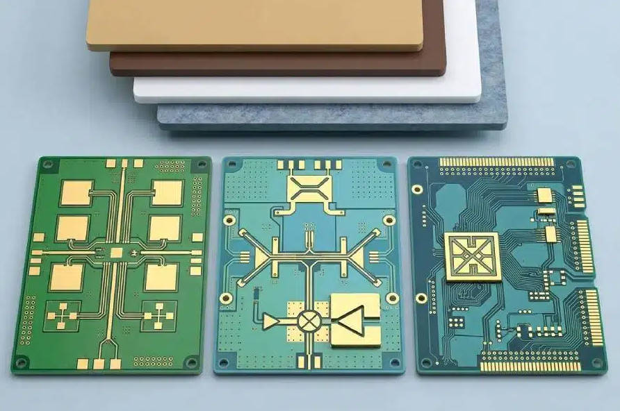
Material Selection for High-Speed AI and GPU PCBs
Standard FR-4 may be suitable for some lower-speed or cost-sensitive sections, but high-speed AI and GPU boards often require materials with better electrical performance.
Important material properties include:
| Material Property | Why It Matters |
|---|---|
| Dielectric constant, Dk | Affects impedance and signal propagation |
| Dissipation factor, Df | Affects signal loss at high frequencies |
| Dk stability | Helps maintain predictable impedance |
| Thermal conductivity | Supports heat management |
| Tg | Indicates thermal stability under assembly and operation |
| CTE | Affects reliability during thermal cycling |
| Copper roughness | Influences insertion loss at high frequencies |
For AI and GPU systems, PCB material selection should be based on signal speed, channel length, loss budget, thermal requirement, and manufacturing cost—not only on board thickness or layer count.
In many applications, hybrid stackups may be used. For example, high-speed signal layers may use lower-loss materials, while less critical layers may use conventional materials to manage cost.
Controlled Impedance in AI and GPU PCB Manufacturing
Controlled impedance is essential for many GPU-related signals, including PCIe, high-speed memory, clock lines, Ethernet, and differential SerDes channels.
A controlled impedance PCB requires coordination between the designer and manufacturer. The manufacturer must understand:
- Target impedance values
- Single-ended or differential impedance
- Layer assignment
- Trace width and spacing
- Reference plane location
- Material type
- Copper thickness
- Impedance tolerance
- Test coupon requirements
Example controlled impedance table:
| Signal Group | Structure | Common Impedance Type | Manufacturing Focus |
|---|---|---|---|
| PCIe lanes | Differential pair | Differential impedance | Loss, skew, via design |
| High-speed clock | Single-ended or differential | 50 Ω or differential value | Low jitter, clean reference |
| Ethernet SerDes | Differential pair | Differential impedance | Crosstalk and insertion loss |
| Memory signals | Single-ended and grouped buses | Interface-specific | Length matching, reference continuity |
| RF/control paths | Microstrip or coplanar | Usually single-ended | EMI and loss control |
When working with Mars PCB’s high-speed PCB manufacture service, controlled impedance requirements can be reviewed with stackup, material, routing, and fabrication tolerances in mind.
AI/GPU PCB Design vs Standard PCB Design
| Item | Standard PCB | High-Speed PCB for AI/GPU Systems |
|---|---|---|
| Signal speed | Low to moderate | High-speed digital, SerDes, PCIe, memory |
| Stackup | Simple 2–6 layers in many products | Often multilayer, impedance-controlled |
| Material | Standard FR-4 often sufficient | Low-loss or high-performance materials may be needed |
| Routing | General trace routing | Transmission line design |
| Impedance control | Often not required | Usually required for critical signals |
| Via design | General vias | Backdrilling, microvias, optimized transitions may be needed |
| Power design | Moderate current | High current, fast transient response |
| Thermal design | Basic thermal relief | Thermal vias, copper balancing, heat spreading |
| Manufacturing review | Basic DFM | DFM + stackup + impedance + SI/PI awareness |
This comparison shows why AI and GPU PCBs should be treated as specialized engineering products rather than ordinary circuit boards.
Engineering Recommendations Before PCB Manufacturing
1. Define High-Speed Interfaces Early
List all high-speed interfaces before layout begins. Include PCIe, memory, Ethernet, clock lines, RF paths, and board-to-board connectors.
2. Confirm the Stackup Before Routing
Do not route first and ask for impedance later. The stackup determines trace width, spacing, dielectric height, and impedance control capability.
3. Use Short, Clean High-Speed Paths
Keep high-speed traces as short and direct as practical. Avoid unnecessary vias, sharp discontinuities, and poorly referenced layer transitions.
4. Maintain Reference Plane Continuity
High-speed traces need continuous return paths. Avoid routing across plane splits or voids. Reference plane discontinuity can create EMI and impedance problems.
5. Control Differential Pair Skew
Differential pairs should be length matched according to interface requirements. However, avoid excessive serpentine routing that creates coupling and impedance distortion.
6. Review Via Transitions
At high speeds, vias are not simple vertical connections. They can create inductance, capacitance, stubs, and reflections. For very high-speed channels, via optimization or backdrilling may be required.
7. Plan Thermal and Power Layout Together
Power integrity and thermal performance are closely linked. High current paths, VRM placement, copper thickness, and heat dissipation must be considered together.
8. Communicate Manufacturing Requirements Clearly
Send the PCB manufacturer a clear package including stackup, impedance table, material requirements, Gerber or ODB++ files, drill data, and special notes.
A professional high-speed PCB design and manufacturing partner can help identify risks before fabrication, reducing the chance of expensive redesigns.
Common Mistakes in AI and GPU PCB Projects
Mistake 1: Treating High-Speed PCB as a Normal Multilayer PCB
A multilayer PCB is not automatically a high-speed PCB. High-speed performance depends on stackup design, impedance control, materials, return paths, and manufacturing stability.
Mistake 2: Choosing Materials Only by Cost
Low-cost material may be acceptable in some sections, but high-loss material can reduce signal margin in long or fast channels. Material choice should match the interface speed and channel length.
Mistake 3: Ignoring Power Integrity Until Testing
Power integrity problems are often difficult to fix after fabrication. Decoupling, plane design, and VRM layout should be planned from the beginning.
Mistake 4: Overlooking Manufacturing Tolerances
A design may pass simulation but fail in production if trace width, dielectric thickness, copper plating, or registration tolerances are not considered.
Mistake 5: Not Involving the PCB Manufacturer Early
For AI and GPU systems, early DFM and stackup review can prevent routing changes, material conflicts, and impedance mismatch.
How to Choose a High-Speed PCB Supplier for AI and GPU Systems
When selecting a supplier, buyers should evaluate technical capability, not only price.
| Supplier Capability | Why It Matters |
|---|---|
| High-speed stackup engineering | Ensures routing rules match manufacturable layer construction |
| Controlled impedance manufacturing | Supports PCIe, SerDes, memory, and clock signal requirements |
| Low-loss material options | Reduces insertion loss for high-speed channels |
| HDI and fine-pitch capability | Supports GPU, FPGA, ASIC, and dense memory breakout |
| Thermal and copper management | Improves reliability in high-power designs |
| DFM review | Reduces prototype failure risk |
| Impedance testing support | Provides verification for critical boards |
| Prototype-to-production support | Helps scale from validation to volume manufacturing |
For AI accelerator cards, GPU modules, edge AI boards, and high-performance computing systems, Mars PCB provides custom high-speed PCB manufacturing support for projects requiring controlled impedance, multilayer stackups, and engineering-oriented production review.
FAQ
1. What is a high-speed PCB in AI and GPU systems?
A high-speed PCB in AI and GPU systems is a printed circuit board designed to carry fast digital signals, high-speed differential pairs, memory interfaces, and high-current power rails while maintaining signal integrity, power integrity, and thermal reliability.
2. Why do GPU boards need controlled impedance PCB design?
GPU boards need controlled impedance because interfaces such as PCIe, memory buses, clocks, and SerDes links are sensitive to reflections and signal distortion. Controlled impedance helps maintain predictable signal transmission across the PCB.
3. What PCB materials are commonly used for AI hardware?
AI hardware may use standard FR-4 for less critical sections, but high-speed channels often require lower-loss materials with stable Dk and Df values. The final material depends on signal speed, channel length, thermal requirements, and cost targets.
4. How many layers does a GPU PCB need?
There is no fixed layer count for all GPU PCBs. Many GPU and AI boards use multilayer stackups to support controlled impedance, dense routing, power planes, and ground planes. The required layer count depends on component density and interface complexity.
5. What is the biggest PCB design challenge in AI accelerator cards?
The biggest challenge is balancing signal integrity, power integrity, thermal performance, and manufacturability in one compact design. High-speed routing, high-current power delivery, and dense GPU or FPGA packages must be planned together.
6. Do AI and GPU PCBs require impedance testing?
Many AI and GPU PCBs with critical high-speed signals require impedance verification, especially for PCIe, SerDes, Ethernet, and clock lines. Whether testing is required depends on the product specification and reliability requirements.
7. How should I choose a high-speed PCB manufacturer for GPU systems?
Choose a manufacturer that can support stackup review, controlled impedance, low-loss materials, HDI fabrication, DFM analysis, impedance testing, and prototype-to-production manufacturing for high-speed PCB projects.
Conclusion
AI and GPU systems place demanding requirements on PCB design and manufacturing. The board must support high-speed data paths, dense component routing, stable power delivery, and reliable thermal performance. As PCIe, memory, SerDes, and GPU interconnect speeds continue to increase, PCB design becomes a critical part of system-level performance.
A successful high-speed PCB for AI and GPU systems requires early stackup planning, controlled impedance, low-loss material selection, reliable power distribution, and close cooperation with the PCB manufacturer.
If your project involves GPU accelerator cards, AI servers, edge AI modules, or high-performance computing hardware, Mars PCB can support high-speed PCB solutions from design review and stackup planning to custom PCB manufacturing.