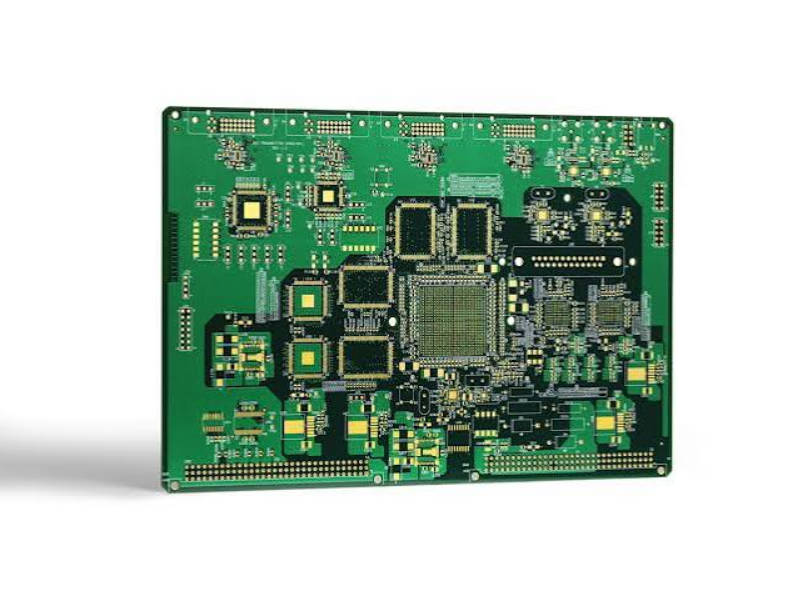
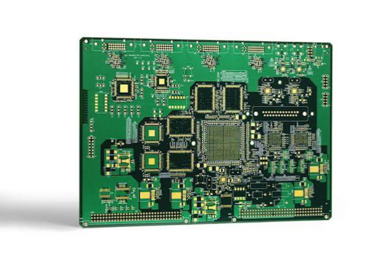
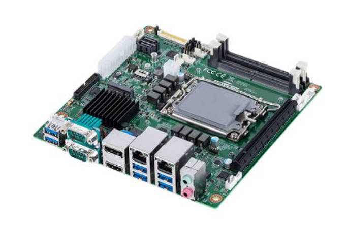
RF PCB manufacturing requires tighter control of material properties, stackup design, impedance, copper surface, via structure, and fabrication tolerance than standard PCB production. Before fabrication, engineers should confirm the operating frequency, target impedance, laminate type, copper roughness, dielectric thickness, via transition design, surface finish, and test requirements with the PCB manufacturer.
For RF and high-frequency circuits, a small variation in dielectric constant, trace width, copper profile, or layer registration can affect insertion loss, phase stability, return loss, and antenna performance. This is why RF PCB fabrication should not be treated as a normal FR-4 PCB order with a different material name.
This guide explains what engineers should check before sending an RF PCB design for fabrication, how manufacturing choices affect RF performance, and how to communicate requirements clearly with a PCB supplier. For projects that require high-frequency materials and RF-focused fabrication support, Mars-PCB provides high-frequency RF PCB manufacturing for applications such as communication circuits, wireless devices, radar systems, and other high-speed electronics.
What Is an RF PCB?
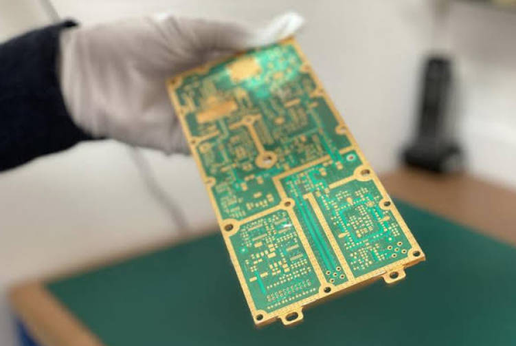
An RF PCB is a printed circuit board designed to transmit radio-frequency signals with controlled electrical behavior. These boards are commonly used in wireless communication, RF modules, antennas, radar electronics, microwave circuits, satellite communication, automotive radar, test equipment, and high-speed data systems.
In standard digital or low-frequency PCB designs, the main concerns may include routing density, power integrity, thermal reliability, and manufacturability. In RF PCB manufacturing, the board itself becomes part of the signal path. The dielectric material, copper foil, trace geometry, ground reference, via transitions, and surface finish all influence electrical performance.
The main purpose of an RF PCB is to preserve signal integrity by controlling impedance, minimizing signal loss, and reducing unwanted radiation or coupling.
RF PCBs often use materials with lower dielectric loss than standard FR-4. Depending on frequency, power, cost target, and mechanical requirements, engineers may choose Rogers materials, PTFE-based laminates, ceramic-filled materials, specialized low-loss FR-4, Taconic materials, or hybrid stackups that combine RF laminates with conventional PCB materials.
Why RF PCB Manufacturing Is Different from Standard PCB Fabrication
RF circuits are sensitive to physical variation. At high frequencies, a PCB trace behaves as a transmission line rather than a simple conductor. This means that the fabricated board must closely match the simulated or calculated design.
For example, if a 50-ohm microstrip line is designed based on a specific dielectric thickness and dielectric constant, the actual trace width, copper thickness, solder mask condition, and material tolerance must be controlled during production. Otherwise, the fabricated board may not match the intended impedance.
In RF PCB fabrication, manufacturing tolerance is not only a mechanical issue; it directly affects electrical performance.
Several factors make RF PCB manufacturing more demanding:
| Factor | Standard PCB Concern | RF PCB Concern |
| Material | Mechanical strength, cost, Tg | Dk stability, Df, loss, thermal expansion |
| Trace width | Current capacity, routing density | Impedance, phase response, insertion loss |
| Copper foil | Conductivity, plating quality | Surface roughness, skin effect loss |
| Stackup | Layer count, manufacturability | Field control, impedance, return path |
| Via design | Connectivity and reliability | Stub effect, inductance, RF transition loss |
| Surface finish | Solderability | RF loss, flatness, oxidation control |
| Fabrication tolerance | Yield and assembly fit | Frequency response and repeatability |
For this reason, engineers should involve the PCB manufacturer before finalizing the stackup. A design that looks correct in simulation may become unstable if the chosen laminate, copper type, prepreg thickness, or trace tolerance is not available in actual production.
Key RF PCB Manufacturing Factors Engineers Should Check
1. Operating Frequency and Signal Type
The first step is to define the operating frequency range. A board designed for sub-GHz wireless communication may not require the same material or via strategy as a microwave circuit operating at several GHz or higher.
Engineers should clarify:
- Operating frequency range
- Analog RF, microwave, high-speed digital, or mixed-signal behavior
- Target impedance, commonly 50 ohms for RF transmission lines
- Power level and thermal load
- Antenna, filter, amplifier, or interconnect function
- Required insertion loss, return loss, or phase stability targets
The higher the operating frequency, the more important material loss, copper roughness, via transition quality, and impedance tolerance become.
This does not mean every RF project needs the most expensive laminate. It means the material and stackup should match the actual electrical requirement, not just the phrase “high frequency.”
2. Material Selection: Dk, Df, and Dimensional Stability
Material selection is one of the most important decisions in RF PCB manufacturing. The dielectric constant, usually called Dk, affects signal propagation speed and impedance calculation. The dissipation factor, usually called Df, affects dielectric loss.
A lower Df is generally preferred for RF and microwave circuits because it helps reduce signal loss. A stable Dk is also important because variation can shift impedance and phase response.
Common RF PCB material options include:
| Material Type | Common Use | Advantages | Considerations |
| High-frequency FR-4 | Lower-frequency RF, cost-sensitive designs | Lower cost, familiar processing | Higher loss than dedicated RF laminates |
| Rogers materials | RF, microwave, antennas, communication modules | Stable electrical properties, low loss options | Higher cost than standard FR-4 |
| PTFE-based laminates | Microwave and high-frequency circuits | Very low dielectric loss | More demanding fabrication process |
| Ceramic-filled PTFE | RF circuits requiring stability | Improved dimensional and thermal stability | Material and processing cost |
| Taconic materials | RF and microwave applications | Low-loss options for specialized designs | Availability and stackup compatibility should be confirmed |
| Hybrid stackup | RF layer + digital/control layers | Balances RF performance and cost | Requires careful lamination and CTE planning |
Mars-PCB’s high-frequency PCB page lists material categories such as Rogers, Taconic, PTFE/Teflon-based materials, ceramic-filled PTFE composites, LCP, polyimide, and low-loss prepregs for high-frequency applications. (Mars)
When discussing material selection with a supplier, engineers should not only ask, “Do you support Rogers PCB manufacturing?” A better question is: “Which material, dielectric thickness, copper type, and stackup can you manufacture repeatedly for this impedance and frequency range?”
3. Stackup Design and Controlled Impedance
RF PCB stackup design determines how electromagnetic fields are controlled. For microstrip, stripline, coplanar waveguide, and grounded coplanar waveguide structures, impedance depends on trace width, dielectric thickness, copper thickness, Dk, solder mask, and ground reference.
A reliable RF PCB stackup should define:
- Layer arrangement
- RF signal layer
- Reference ground plane
- Dielectric thickness
- Copper thickness
- Target impedance
- Impedance tolerance
- Solder mask condition over RF traces
- Special requirements for coplanar waveguide or via fences
Controlled impedance should be defined before fabrication, not corrected after the PCB has already been produced.
For many RF layouts, 50-ohm single-ended transmission lines are common, but the correct target depends on the circuit design. Some systems may use 75-ohm lines, differential impedance, or application-specific impedance values.
Before ordering, engineers should ask the PCB manufacturer to verify whether the stackup can meet the required impedance with manufacturable trace widths and spacing. If the calculated line width is too narrow or too close to adjacent copper, yield and repeatability may become problems.
4. Copper Roughness and Conductor Loss
At high frequency, current tends to concentrate near the surface of the conductor due to skin effect. This makes copper surface roughness more important than in low-frequency designs.
Rough copper can increase conductor loss, especially in microwave and high-speed applications. For this reason, RF PCB manufacturing may require smoother copper foil, careful material selection, and controlled treatment processes.
Engineers should check:
- Rolled copper or electrodeposited copper options
- Copper roughness profile
- Copper thickness after plating
- Whether the RF trace requires specific copper treatment
- Whether insertion loss is sensitive to conductor roughness
For cost-sensitive RF designs, standard copper may still be acceptable. For higher-frequency or low-loss designs, copper roughness should be reviewed early because it may affect material choice, price, and availability.
5. Via Design, Via Stubs, and RF Transitions
Vias are often necessary for grounding, layer transitions, shielding, and interconnection. However, in RF circuits, vias are not electrically invisible. A via can introduce inductance, capacitance, discontinuity, and resonance.
Important via-related checks include:
- Via diameter and pad size
- Via-to-ground spacing
- Via fence pitch near RF traces
- Layer transition structure
- Back-drilling requirement
- Blind or buried via feasibility
- Thermal via placement for RF power devices
- Ground via density around RF components
If a high-frequency signal changes layers through a via, the transition should be designed carefully. For very high-frequency designs, unused via barrels may act as stubs and affect signal quality. In such cases, back-drilling or alternative via structures may be considered.
In RF PCB design for manufacturing, every via in the signal path should be treated as part of the RF structure, not just as a vertical connection.
6. Grounding, Shielding, and Return Path Control
A stable ground reference is essential for RF PCB performance. Poor ground continuity can cause impedance discontinuity, radiation, crosstalk, and unpredictable EMI behavior.
Engineers should check:
- Continuous ground plane under RF traces
- Short return path
- Ground stitching vias
- Via fences beside coplanar waveguide structures
- Isolation between RF, digital, and power regions
- Cavity, shielding, or edge plating requirements if needed
- Avoidance of split reference planes under critical RF paths
RF signals need a controlled return path. If the return current must detour around plane gaps, slots, or poorly placed cutouts, the circuit may radiate more energy or suffer from degraded signal quality.
For RF modules, antennas, and microwave circuits, grounding strategy should be discussed with both the circuit designer and PCB manufacturer before fabrication.
RF PCB Fabrication Process: What Happens After File Submission
The RF PCB fabrication process generally follows the same broad sequence as standard PCB production, but with more attention to material handling, registration, stackup control, drilling quality, and electrical verification.
| Process Step | Engineering Concern | What to Confirm Before Fabrication |
| DFM review | Manufacturability risk | Minimum trace/space, annular ring, clearances |
| Material preparation | Electrical stability | Laminate type, Dk/Df, copper type, thickness |
| Inner layer imaging | Trace accuracy | RF trace width tolerance |
| Etching | Impedance control | Etch compensation for fine RF lines |
| Lamination | Stackup repeatability | Dielectric thickness and registration |
| Drilling | Via reliability | Aspect ratio, drill tolerance, RF via structure |
| Plating | Copper quality | Hole wall thickness and copper buildup |
| Solder mask | RF performance impact | Mask over or away from RF traces |
| Surface finish | Solderability and RF loss | ENIG, immersion silver, OSP, or other finish |
| Testing | Quality verification | Electrical test, impedance test, optional RF test |
For RF boards, engineers should not skip DFM review. DFM can identify issues such as insufficient copper clearance, problematic via structure, non-manufacturable trace widths, unclear stackup notes, and inconsistent impedance requirements.
Mars-PCB’s broader PCB manufacturing service positioning can be reviewed from the Mars-PCB custom PCB solutions page when evaluating whether the project requires PCB fabrication, assembly, or broader manufacturing support.
RF PCB Surface Finish: What Engineers Should Consider
Surface finish affects solderability, shelf life, assembly compatibility, and in some cases RF performance. Common options include ENIG, immersion silver, OSP, immersion tin, and others depending on supplier capability and project requirements.
For RF applications, engineers should consider:
- Solderability requirements
- Fine-pitch component needs
- Bonding requirements
- Oxidation resistance
- Surface flatness
- Frequency sensitivity
- Cost and availability
- Compatibility with assembly process
ENIG is commonly used in many PCB applications because of its flatness and solderability, but the best choice depends on the circuit, assembly method, and frequency sensitivity. Immersion silver may be considered in some RF applications due to conductivity, but it requires proper handling and storage. The final decision should be confirmed with the PCB manufacturer and assembly team.
Common RF PCB Manufacturing Mistakes
Mistake 1: Choosing Material Only by Brand Name
Using a well-known RF laminate does not automatically guarantee good RF performance. The correct material depends on frequency, loss budget, thermal requirement, mechanical reliability, copper type, and stackup.
A practical approach is to compare materials by Dk, Df, thickness availability, copper type, CTE, processing requirements, and cost.
Mistake 2: Sending Gerber Files Without a Clear Stackup
Gerber files alone may not fully define the RF performance target. Engineers should include a stackup drawing, impedance table, material requirements, copper thickness, surface finish, and special manufacturing notes.
Mistake 3: Ignoring Solder Mask Effects
Solder mask can affect impedance and loss on exposed RF transmission lines. Some RF designs require solder mask clearance over critical RF traces. Others may allow solder mask depending on frequency and tolerance. The requirement should be clearly marked.
Mistake 4: Treating RF Vias Like Standard Signal Vias
A poorly designed via transition can cause reflection, insertion loss, and unwanted resonance. For high-frequency signal transitions, engineers should review via geometry, ground return vias, and possible via stub effects.
Mistake 5: Not Confirming Fabrication Tolerance
Trace width, dielectric thickness, copper plating, and layer registration all affect impedance and RF behavior. Engineers should ask what tolerance the manufacturer can realistically hold for the selected material and stackup.
RF PCB Fabrication Checklist Before Ordering
Before sending files for RF PCB manufacturing, engineers should prepare a clear fabrication package.
| Item to Prepare | Why It Matters |
| Gerber or ODB++ files | Defines copper, mask, silkscreen, and board outline |
| Drill files | Defines plated and non-plated holes |
| Stackup drawing | Defines material, copper, dielectric thickness, and layer order |
| Impedance table | Specifies target impedance and tolerance |
| Material requirement | Prevents unsuitable laminate substitution |
| Copper thickness | Affects impedance, loss, and current handling |
| Surface finish | Affects assembly and RF behavior |
| Solder mask notes | Important for exposed RF traces |
| Controlled depth drilling notes | Needed for back-drilling or special via structures |
| Test requirements | Defines electrical, impedance, or additional inspection needs |
| Assembly notes if required | Helps align fabrication and component mounting requirements |
A complete RF PCB fabrication package reduces engineering back-and-forth, lowers the risk of respins, and helps the manufacturer quote more accurately.
If the project involves high-frequency communication circuits, antennas, microwave modules, or RF power sections, engineers can share project requirements with Mars-PCB’s RF PCB manufacturing team for stackup and manufacturability review.
How to Choose an RF PCB Manufacturer
Choosing an RF PCB manufacturer should not be based only on unit price. The supplier should understand high-frequency materials, controlled impedance, lamination behavior, drilling quality, copper roughness, and RF-related DFM issues.
When evaluating a supplier, ask these questions:
- Which RF materials can you process regularly?
- Can you support the required dielectric thickness and copper weight?
- Can you provide controlled impedance review before fabrication?
- What impedance tolerance can you support for this stackup?
- Can you handle PTFE-based or hybrid stackups if needed?
- How do you control etching and trace width tolerance?
- Can you support via structures required for RF transitions?
- What surface finishes do you recommend for this application?
- Do you provide impedance testing coupons?
- Can you support prototype and later production quantities?
A capable RF PCB supplier should be able to review the design before production and point out risks that may affect manufacturability, cost, or electrical performance.
For engineers comparing suppliers, Mars-PCB high-frequency PCB fabrication is relevant when the project requires low-loss materials, controlled impedance, and PCB manufacturing support for RF or high-speed communication applications.
Cost Factors in RF PCB Manufacturing
RF PCB cost is usually higher than standard FR-4 PCB cost because materials, process control, and yield requirements are more demanding.
Main cost factors include:
| Cost Factor | Why It Affects Price |
| Laminate type | RF materials are usually more expensive than standard FR-4 |
| Layer count | More layers increase lamination and registration complexity |
| Hybrid stackup | Combining RF and FR-4 materials requires process control |
| Tight impedance tolerance | Requires stricter stackup and etching control |
| Fine RF trace geometry | May reduce yield if tolerances are tight |
| Special vias | Blind vias, buried vias, or back-drilling add cost |
| Surface finish | Different finishes have different process costs |
| Testing requirements | Impedance coupons or additional inspection add time |
| Prototype quantity | Small batches have higher unit setup cost |
The lowest quote is not always the most economical option if the board later requires redesign or re-fabrication. For RF circuits, early DFM review and accurate stackup confirmation often save more cost than choosing a lower-priced but unsuitable process.
FAQ
What is RF PCB manufacturing?
RF PCB manufacturing is the fabrication of printed circuit boards designed for radio-frequency signals. It requires controlled impedance, low-loss materials, stable stackup construction, precise trace geometry, and careful via and grounding design to maintain signal integrity.
What material is commonly used for RF PCB fabrication?
Common RF PCB materials include Rogers laminates, PTFE-based materials, ceramic-filled PTFE, Taconic materials, high-frequency FR-4, and hybrid stackups. The right material depends on frequency, signal loss target, power level, cost, and mechanical requirements.
Why is controlled impedance important in RF PCB manufacturing?
Controlled impedance helps RF signals travel through PCB traces with minimal reflection and distortion. If impedance is not controlled, the circuit may experience signal loss, return loss, EMI issues, or degraded antenna and microwave performance.
Is FR-4 suitable for RF PCB design?
FR-4 may be suitable for some lower-frequency or cost-sensitive RF designs, especially when loss requirements are not strict. For higher-frequency or low-loss applications, dedicated RF laminates are often preferred because they provide more stable Dk and lower Df.
What should engineers send to an RF PCB manufacturer before fabrication?
Engineers should provide Gerber or ODB++ files, drill files, stackup drawing, impedance table, material requirements, copper thickness, surface finish, solder mask notes, via requirements, and test requirements. A complete fabrication package helps reduce production risk.
How do I choose an RF PCB manufacturer?
Choose an RF PCB manufacturer that understands high-frequency materials, impedance control, RF stackup design, copper roughness, via transitions, and DFM review. The supplier should be able to verify manufacturability before production.
What affects the cost of RF PCB fabrication?
RF PCB fabrication cost is affected by laminate type, layer count, controlled impedance tolerance, hybrid stackup complexity, special via structures, surface finish, testing requirements, and order quantity.
Conclusion
RF PCB manufacturing is not only about producing a circuit board with an RF material. It requires coordinated control of material selection, stackup design, impedance, copper roughness, via transitions, grounding, surface finish, and fabrication tolerance.
For engineers, the safest approach is to confirm the design and manufacturing requirements before fabrication begins. A clear stackup, complete impedance table, suitable material selection, and early DFM review can reduce the risk of signal loss, impedance mismatch, production delay, and costly respins.
If your project involves RF communication circuits, high-frequency modules, antennas, radar electronics, or microwave applications, Mars-PCB can help review your requirements and support RF PCB manufacturing for high-frequency applications.