Low Dk and low Df PCB materials are high-frequency laminates designed to support faster signal propagation, lower signal loss, and more stable impedance in RF, microwave, radar, antenna, and high-speed circuit boards. Dk refers to dielectric constant, which affects signal speed and impedance. Df refers to dissipation factor, also called loss tangent, which affects how much signal energy is lost inside the dielectric material.
For high-frequency PCB design, Dk and Df are not just datasheet numbers. They influence trace width, controlled impedance, insertion loss, phase stability, antenna tuning, and whether a design can perform consistently after fabrication.
In simple terms: Dk tells engineers how the material changes the electric field and signal speed; Df tells engineers how much signal energy is converted into heat as the signal travels through the PCB material.
Mars-PCB supports low Dk and low Df PCB materials for high-frequency PCB and RF PCB projects where material selection, impedance control, and fabrication stability are critical.
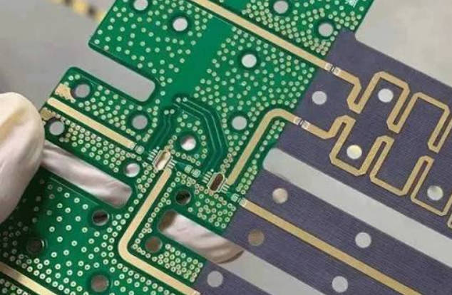
Dk and Df Explained in Plain Engineering Terms
Before choosing high-frequency PCB materials, engineers need to separate two related but different questions.
First: how fast and in what geometry will the signal travel?
Second: how much signal energy will be lost during transmission?
Dk helps answer the first question. Df helps answer the second.
| Parameter | Full Name | Also Called | Main Effect in PCB Design |
| Dk | Dielectric Constant | Relative permittivity, Er | Affects signal speed, impedance, wavelength, and trace geometry |
| Df | Dissipation Factor | Loss tangent, tan δ | Affects dielectric loss and insertion loss |
Dk affects how the signal behaves geometrically. Df affects how much signal energy the material absorbs.
This distinction matters because a material can have a suitable Dk but still have too much loss for a high-frequency application. Similarly, a very low Df material may not be practical if its Dk, thickness, cost, or fabrication behavior does not fit the stackup.
What Is Dk in PCB Materials?
Dk, or dielectric constant, describes how much a PCB material slows down an electromagnetic signal compared with air or vacuum. In PCB design, it affects signal velocity, impedance, and the physical size of RF structures.
A lower Dk generally allows faster signal propagation and larger wavelength inside the PCB material. A higher Dk slows the signal more and can make RF structures physically smaller.
For example, in RF antennas, filters, and microwave circuits, Dk can affect the length of transmission lines, antenna dimensions, and resonant behavior. In controlled impedance routing, Dk affects how wide a trace must be to reach a target impedance such as 50 ohms.
How Dk Affects PCB Design
| Design Area | Effect of Dk |
| Signal speed | Lower Dk usually supports faster propagation |
| Impedance | Dk influences trace width needed for target impedance |
| RF wavelength | Higher Dk shortens wavelength inside the material |
| Antenna size | Higher Dk can reduce physical size, but may affect bandwidth |
| Phase stability | Dk variation can shift phase response |
| Stackup design | Dk affects dielectric thickness and trace geometry decisions |
For RF and high-speed PCB design, stable Dk is often more important than simply choosing the lowest Dk.
A very low Dk material is not automatically the right choice. Engineers must check whether the Dk value is stable across frequency, temperature, thickness, and production batches. In many RF applications, consistency matters as much as the nominal value.
What Is Df in PCB Materials?
Df, or dissipation factor, describes how much signal energy is lost in the dielectric material. It is also commonly called loss tangent.
When a high-frequency signal travels through a PCB transmission line, part of the energy is lost in the conductor and part is lost in the dielectric material. Df is related to dielectric loss. A lower Df generally means less energy is absorbed by the material.
This is why low Df PCB materials are important for RF, microwave, radar, antenna, and high-speed communication applications.
How Df Affects PCB Design
| Design Area | Effect of Df |
| Insertion loss | Lower Df helps reduce dielectric loss |
| Signal integrity | Lower loss supports cleaner high-frequency transmission |
| Heat generation | Lower dielectric loss can reduce energy converted to heat |
| Long trace routing | Loss becomes more important over longer paths |
| High-frequency operation | Df becomes increasingly important as frequency rises |
| Radar and antenna systems | Lower loss can help preserve RF signal strength |
Df is especially important when the signal frequency is high, the trace length is long, or the loss budget is tight.
For short, lower-frequency traces, Df may not dominate the design. For microwave circuits, radar front ends, high-speed backplanes, and RF antennas, Df can become a major material selection factor.
Low Dk vs Low Df: They Are Not the Same Thing
Many people mention “low Dk low Df PCB” as if the two values always move together. In practice, Dk and Df describe different material behaviors.
| Question | Related Parameter |
| How fast does the signal travel? | Dk |
| What trace width is needed for impedance? | Dk + dielectric thickness + copper geometry |
| How much dielectric loss occurs? | Df |
| Will insertion loss be acceptable? | Df + copper loss + trace length |
| Will phase remain consistent? | Dk stability |
| Will the material support low-loss RF design? | Mainly Df, but also copper roughness and stackup |
A material with low Dk may help with signal speed and certain RF geometries, but if its Df is not low enough, signal loss may still be too high. A material with low Df may reduce loss, but if the Dk is not appropriate for the design, impedance and layout geometry may become difficult.
The correct approach is to evaluate Dk, Df, thickness, copper roughness, thermal behavior, material availability, and fabrication capability together.
Why Low Dk and Low Df Matter in High-Frequency PCB Materials
At higher frequencies, PCB material behavior becomes more visible in real circuit performance. What looks like a small material difference on a datasheet can become important in RF testing.
Low Dk and low Df materials are commonly considered when a PCB must support:
- RF communication modules
- Microwave circuits
- Radar systems
- Antenna arrays
- Satellite communication equipment
- High-speed digital transmission
- 5G-related RF circuits
- Test and measurement equipment
- Automotive electronics
- Low-loss interconnects
For these applications, engineers often care about insertion loss, return loss, impedance control, phase matching, crosstalk, and repeatability.
Mars-PCB provides high-frequency PCB material support for projects that require low-loss materials, controlled impedance, and RF-focused fabrication review.
How Dk Affects Controlled Impedance
Controlled impedance is one of the most common reasons engineers pay attention to Dk.
In a PCB transmission line, impedance depends on several variables:
| Variable | Role in Impedance |
| Dk | Affects electromagnetic field behavior |
| Dielectric thickness | Distance between trace and reference plane |
| Trace width | Main geometry variable for impedance |
| Copper thickness | Changes effective conductor shape |
| Solder mask | Can affect outer-layer impedance |
| Ground reference | Defines return path and field structure |
| Etching tolerance | Changes final trace width |
For a 50-ohm RF trace, the same trace width will not produce the same impedance on every material. If the Dk changes, the required trace width also changes.
This is why the PCB manufacturer should confirm the stackup before layout is finalized. If engineers design the board using one Dk value but the manufacturer uses a different material or thickness, the impedance may shift.
In controlled impedance PCB design, Dk is only useful when it is tied to a real manufacturable stackup.
How Df Affects Signal Loss
Df contributes to dielectric loss. In high-frequency PCBs, total signal loss usually includes dielectric loss, conductor loss, radiation loss, and discontinuity loss. Df mainly relates to the dielectric portion.
As frequency rises, dielectric loss becomes more important. This is why low Df materials are often used in microwave PCB fabrication, radar PCB design, RF antenna boards, and high-speed communication circuits.
However, Df is not the only loss factor. Engineers should also consider:
- Copper roughness
- Finished copper thickness
- Trace length
- Via transitions
- Connector launches
- Surface finish
- Solder mask
- Impedance discontinuities
- Stackup quality
A low Df laminate cannot fully compensate for poor routing, long stubs, weak grounding, rough copper, or uncontrolled impedance. Material selection and PCB design must work together.
Typical Material Categories for Low Dk and Low Df PCB Designs
Different projects require different material strategies. The table below gives a practical overview.
| Material Category | Typical Use Direction | Main Advantage | Key Check Before Fabrication |
| Low-loss RF laminates | RF, microwave, antenna, radar boards | Lower dielectric loss and stable RF behavior | Exact material grade, Dk/Df, thickness, copper type |
| PTFE-based materials | Low-loss microwave and RF circuits | Low dielectric loss in many applications | Processing difficulty, drilling, bonding, cost |
| Ceramic-filled PTFE | Stable RF and microwave designs | Better dimensional or thermal stability than some pure PTFE systems | CTE, lamination, availability |
| Hydrocarbon ceramic laminates | Commercial RF and microwave boards | Balance between RF performance and manufacturability | Stackup, copper, impedance tolerance |
| Low-loss FR-4 alternatives | Cost-sensitive high-speed or lower RF applications | Lower cost than many RF laminates | Loss performance at actual frequency |
| Hybrid stackups | RF layer + digital/control layers | Balances cost and RF performance | Material compatibility and lamination control |
The material decision should not start with “which is the best.” It should start with: what frequency, what impedance, what loss limit, what stackup, what quantity, and what production target?
When Do You Really Need Low Dk Low Df PCB Materials?
Not every PCB needs low Dk and low Df materials. For low-speed control circuits, standard FR-4 may be sufficient. For lower-frequency RF or short signal paths, cost-performance materials may be acceptable.
Low Dk and low Df materials become more important when:
| Situation | Why Material Matters |
| High operating frequency | Loss and impedance variation become more visible |
| Long RF or high-speed traces | More length means more accumulated loss |
| Tight insertion loss requirement | Df becomes a key design factor |
| Radar or antenna design | Dk stability affects tuning and phase |
| High-speed differential links | Material loss affects eye diagram and signal margin |
| Phase-sensitive circuits | Dk consistency affects timing and phase |
| Production repeatability needed | Material tolerance affects batch consistency |
If the project is only cost-sensitive and not electrically demanding, using advanced material may increase cost without meaningful benefit. If the project is performance-sensitive, using unsuitable material may cause expensive redesign.
Common Mistakes When Reading Dk and Df Values
Mistake 1: Comparing Dk Values Without Checking Test Frequency
Dk can be measured under different test conditions. A value listed at one frequency may not be directly comparable to another material tested differently. Engineers should check the datasheet conditions and ask the PCB supplier how the value is used in impedance calculation.
Mistake 2: Thinking Lower Dk Is Always Better
Lower Dk can support faster signal speed, but it may also change trace geometry and physical circuit size. Some RF designs may intentionally use a higher Dk material to reduce antenna or circuit size. The right Dk depends on the design goal.
Mistake 3: Ignoring Dk Tolerance
The nominal Dk value is not enough. Dk tolerance and stability affect impedance and repeatability. For phase-sensitive RF circuits, variation may matter more than the headline number.
Mistake 4: Looking Only at Df and Ignoring Copper Roughness
Df affects dielectric loss, but conductor loss also matters. At high frequency, copper roughness can significantly influence insertion loss. A low Df material with unsuitable copper may not perform as expected.
Mistake 5: Selecting Material Before Confirming Fabrication Capability
Some high-frequency materials require special processing. Before finalizing material choice, engineers should confirm whether the PCB supplier can process the laminate, thickness, copper type, and stackup consistently.
What to Tell Your PCB Supplier When Asking About Low Dk and Low Df Materials
A material request such as “please quote low Dk low Df PCB” is too vague. The supplier needs project context to recommend a suitable material and stackup.
Prepare the following information:
| Information to Provide | Why It Helps |
| Operating frequency | Determines material loss requirement |
| Signal type | RF, microwave, high-speed digital, antenna, radar |
| Target impedance | Needed for stackup and trace geometry |
| Stackup requirement | Defines material thickness and layer structure |
| Preferred material | Helps quote exact laminate if already selected |
| Acceptable alternatives | Allows cost-performance comparison |
| Insertion loss requirement | Helps judge whether Df is critical |
| Thermal environment | Affects material and reliability choice |
| Surface finish requirement | Important for assembly and RF behavior |
| Quantity and project stage | Prototype and production may need different planning |
For early-stage projects, Mars-PCB can help review RF PCB material selection based on frequency, impedance, stackup, and fabrication requirements.
Practical Selection Guide: Dk, Df, or Both?
The following guide helps engineers decide which parameter deserves more attention.
| Project Situation | Focus More On | Reason |
| 50-ohm RF transmission line | Dk + stackup | Impedance depends on material and geometry |
| Long microwave path | Df + copper roughness | Loss accumulates over distance |
| Antenna PCB | Dk stability | Tuning and radiation pattern depend on material behavior |
| High-speed differential pair | Df + Dk consistency | Loss and impedance both matter |
| Compact RF circuit | Dk | Higher or controlled Dk may support smaller structures |
| Radar or phase-sensitive design | Dk stability + Df | Phase consistency and low loss are both important |
| Cost-sensitive lower-frequency design | Balanced material choice | Advanced low-loss material may not be necessary |
The best material is not the one with the lowest Dk or Df on paper; it is the one that meets the electrical target and can be manufactured consistently.
How Mars-PCB Supports High-Frequency PCB Material Decisions
In high-frequency PCB fabrication, material selection should connect directly to manufacturing. A laminate that looks good in a datasheet must still be available in the right thickness, copper weight, and stackup format.
Mars-PCB can support engineering teams by reviewing:
- RF or high-speed application requirements
- Material options such as Rogers, Taconic, Isola, PTFE-based laminates, and low-loss alternatives
- Controlled impedance stackup
- Dielectric thickness and copper thickness
- Surface finish
- Via and grounding requirements
- DFM risks before fabrication
For broader PCB manufacturing needs beyond RF material selection, engineers can also review Mars-PCB custom PCB manufacturing for project-level fabrication support.
FAQ
What does Dk mean in PCB materials?
Dk means dielectric constant. In PCB materials, it affects signal speed, impedance, wavelength, and trace geometry. For RF and high-speed PCBs, stable Dk helps maintain predictable electrical performance.
What does Df mean in PCB materials?
Df means dissipation factor, also called loss tangent. It describes how much signal energy is lost in the dielectric material. Lower Df generally helps reduce dielectric loss in high-frequency PCB applications.
Is low Dk always better for high-frequency PCB materials?
No. Low Dk can support faster signal propagation, but it is not always better. The right Dk depends on impedance, antenna size, stackup, trace geometry, and phase requirements.
Why is low Df important in RF PCB design?
Low Df is important because it reduces dielectric loss. In RF, microwave, radar, and high-speed circuits, lower dielectric loss can help preserve signal quality and reduce insertion loss.
What is the difference between dielectric constant and loss tangent in PCB design?
Dielectric constant, or Dk, affects signal speed and impedance. Loss tangent, or Df, affects how much signal energy is lost in the PCB material. Both are important for high-frequency PCB design.
Can FR-4 be used instead of low Dk low Df PCB materials?
FR-4 may be suitable for low-speed or some lower-frequency applications. For RF, microwave, radar, or high-speed circuits with strict loss and impedance requirements, low Dk and low Df materials are often preferred.
How should I choose low Dk and low Df PCB materials?
Start with operating frequency, target impedance, insertion loss requirement, stackup, thermal environment, and production needs. Then confirm material availability and manufacturability with the PCB supplier.
Conclusion
Low Dk and low Df are two of the most important material parameters in high-frequency PCB design. Dk affects signal speed, impedance, phase, and physical geometry. Df affects dielectric loss and high-frequency signal attenuation.
For engineers, the practical goal is not to choose the lowest possible numbers. The goal is to select a material with suitable Dk, low enough Df, stable thickness, compatible copper, and reliable fabrication behavior for the actual project.
Mars-PCB supports low Dk and low Df PCB materials for RF PCB, microwave PCB, radar PCB, antenna PCB, and other high-frequency circuit board applications that require material review and controlled impedance fabrication.