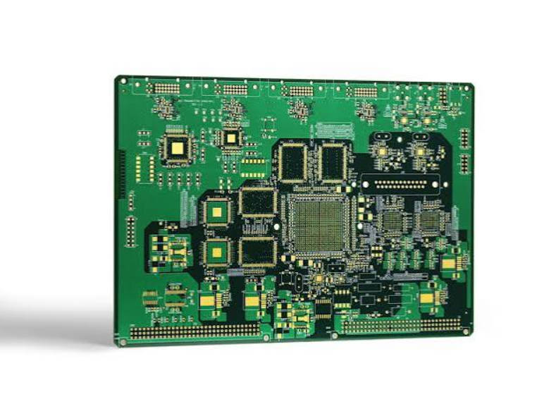
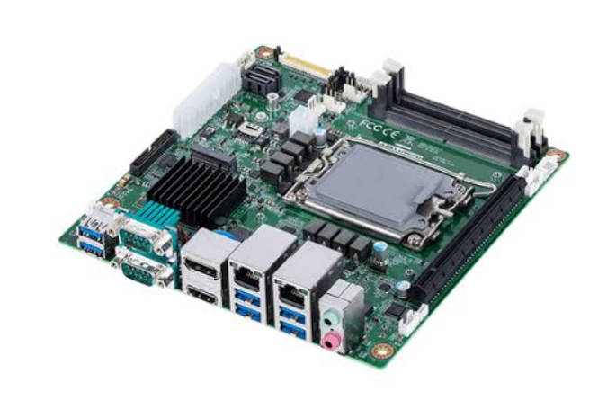
PCIe 7.0 PCB design requires engineers to manage a 128 GT/s PAM4 channel operating at a 32 GHz Nyquist frequency. Compared with PCIe 6.0, the signaling method remains PAM4, but the Nyquist frequency doubles from 16 GHz to 32 GHz. This makes conductor loss, dielectric loss, copper roughness, via stubs, connector transitions and manufacturing variation significantly more influential.
A successful PCIe 7.0 PCB is not created by selecting a low-loss laminate alone; it is created by controlling the complete path from the transmitter package to the receiver package.
The PCIe 7.0 Base Specification Revision 7.0 was officially released on June 11, 2025. It defines a raw data rate of 128 GT/s, PAM4 signaling and up to 512 GB/s of bidirectional bandwidth for an x16 link. (PCI-SIG)
For PCB designers and buyers, this changes the manufacturing conversation. The key question is no longer simply whether a fabricator can produce controlled-impedance differential pairs. The more relevant question is whether the complete material, stackup, routing, via and verification process can preserve the remaining signal-integrity margin at 32 GHz.
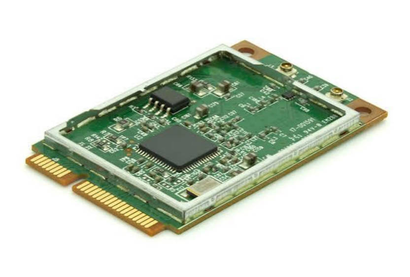
PCIe 7.0 in One Engineering View
| Parameter | PCIe 7.0 Characteristic | PCB Design Impact |
| Raw data rate | 128 GT/s | Higher channel bandwidth and tighter timing margin |
| Signaling | PAM4 | Four voltage levels and three signal eyes |
| Nyquist frequency | 32 GHz | Greater sensitivity to dielectric loss, copper roughness and discontinuities |
| Unit interval | 15.625 ps | Small geometry and timing variations become more significant |
| Maximum x16 bandwidth | Up to 512 GB/s bidirectional | Supports bandwidth-intensive AI, HPC and networking platforms |
| Link encoding | Flit-based encoding with FEC and CRC | Supports reliability while retaining low-latency operation |
| Main PCB challenge | Maintaining the end-to-end channel budget | Requires co-optimization of package, PCB, vias and connectors |
PCI-SIG retained the PAM4 and Flit-mode architecture used by PCIe 6.0. The increase to 128 GT/s is achieved by doubling the clocking and moving from a 16 GHz to a 32 GHz Nyquist frequency. (PCI-SIG)
Checkpoint 1: Build the Channel-Loss Budget Before Routing
A PCIe 7.0 channel is not only the visible differential trace on the motherboard. It may include:
- transmitter silicon and package;
- BGA escape structure;
- plated through-holes or blind vias;
- baseboard routing;
- AC-coupling capacitor pads;
- card-edge or board-to-board connector;
- add-in-card routing;
- receiver package and silicon.
Each section consumes part of the same end-to-end budget.
PCI-SIG’s public technical guidance identifies a die-pad-to-die-pad loss budget of approximately 36 dB at 32 GHz. The same guidance illustrates 9 dB for the root-complex package and 4 dB for the non-root package, leaving approximately 23 dB for the remaining channel elements. The exact allocation still depends on the applicable topology and specification requirements. (PCI-SIG)
The PCB designer should treat insertion loss as a limited system resource that must be allocated, not as a value to be checked after layout is complete.
Typical Channel Contributors
| Channel Element | Primary Risk | Engineering Decision |
| Root-complex package | Package insertion loss and escape constraints | Obtain package models early |
| BGA escape | Neck-down, via transition and return-path discontinuity | Simulate escape and via geometry together |
| Baseboard trace | Dielectric and conductor loss | Select material and copper profile from the required reach |
| AC-coupling capacitor | Pad discontinuity and local impedance change | Optimize pad, anti-pad and reference-plane geometry |
| Connector | Insertion loss, return loss and crosstalk | Use appropriate connector models |
| Add-in card | Additional trace and via loss | Include card routing in the full-channel model |
| Receiver package | Remaining package loss | Use realistic receiver-side package data |
| Manufacturing variation | Impedance and loss distribution | Apply tolerance-based, not nominal-only, simulation |
A common design mistake is to allocate most of the loss budget to the PCB trace and then discover that package and connector models consume more margin than expected. The correct workflow begins with a block-level channel model and gradually replaces estimated elements with measured or supplier-provided models.
Checkpoint 2: Understand What PAM4 Changes
PAM4 transmits four voltage levels rather than the two levels used by NRZ. Each symbol carries two bits and produces three eye openings.
This improves bandwidth efficiency, but the vertical spacing between adjacent levels is smaller. As a result, the receiver has less amplitude margin for noise, reflections and crosstalk. PCI-SIG describes this reduced eye height and eye width as a source of increased error susceptibility and uses Gray coding, precoding, equalization, FEC and CRC to manage the resulting risk.
PAM4 does not merely make the signal faster; it makes small channel imperfections more visible to the receiver.
For the PCB, this increases the importance of:
- impedance continuity;
- low insertion loss;
- low return loss;
- reduced far-end and near-end crosstalk;
- stable reference planes;
- tightly controlled layer transitions;
- low power-distribution noise;
- accurate material models.
Equalization can compensate for predictable frequency-dependent loss. It cannot completely remove deep resonances, strong reflections, severe crosstalk or unexpected manufacturing deviations.
Therefore, the design objective should not be to rely on receiver equalization to rescue a poor interconnect. The objective should be to present the transmitter and receiver with a smooth, modelled and repeatable channel.
Checkpoint 3: Select the PCB Material from the Required Reach
The phrase “PCIe 7.0 material” is too broad to support a technical purchasing decision. The correct material depends on:
- total routed length;
- number of connectors;
- number and type of via transitions;
- copper roughness;
- stackup geometry;
- package loss;
- add-in-card contribution;
- retimer placement;
- operating temperature;
- required production yield.
PCI-SIG’s public electrical guidance indicates that server topologies may require PCB loss of no more than approximately 1 dB per inch at 32 GHz. It also notes that very-low-loss laminate systems combined with minimal copper surface roughness can support this target.
This figure should be treated as a channel-planning reference rather than a universal laminate specification. A short chip-to-chip path may have different requirements from a motherboard-to-add-in-card channel.
Material Evaluation Questions
| Material Question | Why It Matters at 32 GHz | Evidence to Request |
| What is the dissipation factor at relevant frequencies? | Dielectric loss increases with frequency and trace length | Frequency-dependent Df data and test method |
| How stable is the dielectric constant? | Dk affects impedance, delay and skew | Dk data across frequency and resin content |
| Which copper profile is used? | Rougher copper increases conductor loss | Copper roughness classification or profile data |
| What glass styles are available? | Glass weave can cause local Dk differences and skew | Proposed prepreg and core constructions |
| How tightly is dielectric thickness controlled? | Thickness variation changes differential impedance | Finished-thickness tolerance |
| Are multiple material sources qualified? | Substitution may alter Dk, Df and process behavior | Approved material and substitution policy |
| Can the supplier provide loss coupons? | Impedance alone does not prove low insertion loss | Coupon design and test-report format |
Avoid comparing materials only by the nominal Df shown in a data sheet. Df values can vary with test method, frequency, resin percentage and sample construction. The model used in simulation should correspond as closely as possible to the actual production stackup.
Copper Roughness Is Part of the Material Decision
At 32 GHz, conductor loss is affected by more than trace width and copper thickness. The effective path followed by surface current is influenced by the copper profile.
Very rough copper may improve laminate adhesion but can increase high-frequency loss. Lower-profile copper can reduce conductor loss, although the complete material and manufacturing process must still provide adequate adhesion and reliability.
The material conversation should therefore include both laminate properties and copper foil treatment. Specifying an ultra-low-loss resin system while ignoring copper profile may leave a substantial portion of the expected improvement unrealized.
Checkpoint 4: Treat Every Via as a Designed Interconnect
A via is not electrically transparent. It introduces:
- capacitive loading from pads;
- inductance from the barrel;
- coupling to nearby vias;
- return-current disruption;
- impedance variation through the transition;
- possible resonance from an unused stub.
PCI-SIG’s educational comparison for successive generations shows a maximum via-stub example decreasing to approximately 6 mil for PCIe 7.0, compared with 10 mil in the PCIe 5.0 and 6.0 examples. This illustrates the shrinking tolerance for unused via barrel at 32 GHz, although the actual allowable stub must be determined from the channel design and applicable specification.
At PCIe 7.0 speeds, via geometry is a signal-integrity structure, not a drill-table detail added after routing.
Key Via Parameters
The design team should define:
- finished hole diameter;
- pad and anti-pad diameter;
- layer transition depth;
- residual backdrill stub;
- backdrill diameter;
- backdrill depth tolerance;
- nearby ground-via placement;
- differential-via spacing;
- reference-plane transition;
- BGA breakout geometry.
Backdrilling removes the unused portion of a plated through-hole. It can reduce stub resonance, but only when the fabricator has an unambiguous depth reference and a realistic residual-stub tolerance.
A fabrication note that says only “backdrill all high-speed vias” is incomplete. The drawing should identify the drilled side, target layer, drill diameter, maximum residual stub and inspection method.
Blind or buried vias may reduce stub length, but they can add cost, lamination complexity and registration risk. They should be selected from the electrical and manufacturing trade-off rather than assumed to be automatically superior.
Checkpoint 5: Convert the Simulation into Manufacturing Controls
A nominal simulation assumes that every trace, dielectric layer and via is produced at its intended value. Production does not work that way.
For PCIe 7.0 PCB fabrication, the design must be evaluated over realistic process limits.
Fabrication Variables That Affect the Channel
| Fabrication Variable | Electrical Effect | Recommended Control |
| Etched trace width | Changes differential and single-ended impedance | Fabricator-specific impedance compensation |
| Trace thickness | Changes conductor loss and impedance | Confirm finished copper assumptions |
| Dielectric thickness | Changes impedance and coupling | Agree finished stackup tolerances |
| Resin content | Changes effective Dk and Df | Lock core and prepreg constructions |
| Copper roughness | Changes high-frequency conductor loss | Specify approved copper profile |
| Layer registration | Creates pair asymmetry and via offset | Review registration capability |
| Backdrill depth | Changes remaining stub resonance | Define residual-stub limit |
| Drill diameter and plating | Changes via impedance | Include actual fabrication dimensions in models |
| Solder-mask coverage | Changes local impedance | Define whether critical pairs are masked |
| Glass-weave placement | Can contribute to intra-pair skew | Use routing and material mitigation where needed |
Nominal Impedance Is Not Enough
A drawing may specify an 85-ohm differential impedance, but this does not describe the complete acceptance condition.
The fabricator also needs:
- impedance tolerance;
- layer and structure identification;
- coupon geometry;
- test frequency or measurement method;
- whether the value refers to design or finished impedance;
- reporting requirements;
- any separate targets for connector breakouts or neck-down regions.
The final impedance should normally be achieved through collaboration between the PCB designer and fabricator. The fabricator may adjust trace width or spacing to compensate for the actual material construction and etching process.
This collaboration should occur before the production files are formally released, not after the first impedance coupon fails.
Checkpoint 6: Decide on Retimers from the Channel, Not Trace Length
There is no single trace-length value that automatically determines whether a PCIe 7.0 design needs a retimer.
The decision depends on:
- total insertion loss;
- return loss;
- package contribution;
- connector count;
- crosstalk;
- transmitter and receiver capability;
- topology;
- required plug-and-play margin;
- production variation.
PCI-SIG’s public guidance states that a retimer or redriver is not necessarily required when the complete channel remains within the specified loss limits. Retimers are commonly considered for longer-reach, plug-and-play system configurations. (PCI-SIG)
A retimer can divide a long path into separate electrical channels, but it does not eliminate the need to design each channel section correctly.
| Approach | Main Function | Suitable Situation | Limitation |
| Direct electrical channel | Connects endpoints without an extension device | Short, low-loss and well-controlled path | Limited by the complete channel budget |
| Redriver | Provides analog signal conditioning | Channels needing additional equalization margin | Does not fully regenerate timing like a retimer |
| Retimer | Recovers and retransmits the signal | Longer reach or system-level channel segmentation | Adds cost, power, placement and thermal requirements |
| Fly-over cable | Moves part of the path away from lossy PCB routing | Dense systems with difficult board reach | Connectors and transitions still require optimization |
The retimer decision should be made during architecture definition. Adding one after layout is largely complete can create new routing, power, thermal and clocking constraints.
A Practical PCIe 7.0 PCB Development Sequence
1. Define the topology
Document the root complex, endpoint, connector, add-in card, cable and retimer arrangement. Establish which elements belong to each compliance segment.
2. Create a preliminary loss allocation
Estimate package, PCB, via and connector loss at 32 GHz. Reserve margin for modelling uncertainty and manufacturing variation.
3. Select a candidate stackup with the fabricator
Do not build the stackup from generic online material values. Use constructions, copper profiles and dielectric thicknesses that the selected fabricator can obtain and control.
A qualified high-speed PCB manufacturing discussion should begin with the channel target, not only the Gerber files.
4. Model the critical transitions
Use appropriate models for:
- BGA breakouts;
- layer-transition vias;
- AC-coupling capacitor pads;
- connector launches;
- backdrilled structures;
- retimer breakouts.
Three-dimensional electromagnetic analysis may be necessary for geometries that cannot be represented accurately by a simple transmission-line model.
5. Run tolerance-based analysis
Evaluate the channel using realistic variation in line width, dielectric thickness, Dk, copper roughness, registration and residual via stubs.
A design that passes only at nominal values may not provide acceptable volume-production margin.
6. Complete fabrication DFM before release
The high-speed PCB fabrication review should confirm:
- producible trace dimensions;
- material availability;
- finished stackup;
- impedance compensation;
- backdrill limits;
- registration assumptions;
- coupon design;
- test and reporting requirements.
7. Correlate simulations with fabricated data
Use impedance coupons, loss coupons, TDR results, insertion-loss measurements or other agreed validation methods to compare production behavior with the original model.
This correlation can improve both the current build and later design revisions.
Common PCIe 7.0 Design and Purchasing Mistakes
| Mistake | Why It Creates Risk | Better Approach |
| Choosing the laminate after routing | The material may not support the required reach | Build the loss model before fixing the stackup |
| Simulating traces but not vias and connectors | Discontinuities may dominate the remaining margin | Model the complete end-to-end channel |
| Comparing only nominal Df values | Data may use different frequencies and test methods | Compare material data on a consistent basis |
| Specifying impedance without process tolerance | Nominal geometry does not represent production spread | Use tolerance-based impedance requirements |
| Requesting backdrilling without a stub limit | The fabricator lacks a measurable acceptance target | Define side, depth, diameter and residual stub |
| Assuming a retimer corrects every problem | Reflections and local discontinuities still remain | Design each retimed segment as a valid channel |
| Accepting unapproved material substitutions | Dk, Df and copper treatment may change | Require technical approval before substitution |
| Requesting only electrical test continuity | Continuity does not validate high-frequency behavior | Add impedance and channel-specific verification |
How to Evaluate a PCIe 7.0 PCB Supplier
A supplier should be evaluated on its ability to translate electrical requirements into repeatable manufacturing controls.
Before requesting a quotation, prepare the following information:
- target PCIe generation and topology;
- estimated lane lengths;
- differential-impedance requirement;
- preliminary insertion-loss target;
- proposed layer count and finished thickness;
- preferred or permitted material class;
- copper-profile expectations;
- via and backdrill structure;
- connector and package information;
- coupon and report requirements;
- prototype and production quantities.
During supplier review, ask whether the proposed stackup is based on materials and constructions that are routinely processed. Also ask how the fabricator controls impedance, validates backdrill depth and manages material substitutions.
For an early feasibility review, the design team can submit its stackup assumptions and critical interconnect requirements through the Mars-PCB website. A focused review should establish what information is still missing before fabrication begins.
FAQ
What is the Nyquist frequency of PCIe 7.0?
PCIe 7.0 uses PAM4 signaling at 128 GT/s with a 32 GHz Nyquist frequency. This is twice the 16 GHz Nyquist frequency used by PCIe 6.0 PAM4 signaling. (PCI-SIG)
What PCB material is required for PCIe 7.0?
There is no universal material for every PCIe 7.0 design. The selected laminate should satisfy the complete channel-loss target at 32 GHz after accounting for trace length, copper roughness, vias, packages and connectors. Long server channels may require a very-low-loss material system and low-profile copper.
Can standard FR-4 be used for PCIe 7.0 PCB design?
FR-4 describes a broad material family rather than one fixed electrical performance level. A conventional medium-loss FR-4 may be unsuitable for long PCIe 7.0 server channels, while an extremely short channel may have different requirements. The decision should be based on channel simulation and measured material data.
Does PCIe 7.0 require PAM4 PCB design?
Yes. PCIe 7.0 uses four-level PAM4 signaling. The PCB must preserve three signal eyes while controlling insertion loss, return loss, crosstalk, skew and manufacturing variation.
How short should a PCIe 7.0 via stub be?
The allowable stub depends on the via geometry and channel design. PCI-SIG educational material illustrates approximately 6 mil as a PCIe 7.0 channel-improvement example, but the actual limit should be established through modelling and the applicable specification.
Is backdrilling mandatory for PCIe 7.0?
Backdrilling is not automatically mandatory for every channel. It is commonly considered when a through-via leaves an unused stub that creates excessive reflection or resonance. Blind vias, optimized layer transitions or shorter through-vias may provide alternatives.
When does a PCIe 7.0 PCB need a retimer?
A retimer may be needed when the full channel cannot maintain the required loss and signal-integrity margin, or when the architecture requires longer plug-and-play reach. The decision should use end-to-end channel analysis rather than a simple maximum trace-length rule.
How should PCIe 7.0 PCB fabrication be validated?
Validation may include controlled-impedance coupons, TDR measurements, insertion-loss coupons, backdrill inspection and correlation between fabricated structures and simulation models. The test plan should be agreed before production.
Conclusion
PCIe 7.0 PCB design pushes high-speed interconnect engineering into a range where material loss, copper roughness, via geometry and normal fabrication variation can no longer be handled as secondary details.
The most reliable development approach is to begin with the full channel budget, choose a producible stackup, model critical transitions and convert simulation assumptions into measurable fabrication requirements.
The final objective is not simply to manufacture an 85-ohm differential pair, but to manufacture a repeatable 128 GT/s channel with enough margin for the complete system.
When preparing a PCIe 7.0 project, provide the fabricator with the topology, material assumptions, loss target, via structure and verification plan. Early collaboration with a high-speed PCB manufacturing partner can identify stackup and fabrication risks before they become prototype failures.