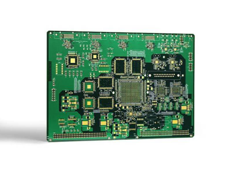
Choose a 2+N+2 HDI stackup when two laser-drilled buildup layers on each side provide enough access to the required routing layers. Choose Any-Layer HDI when fine-pitch packages, limited board area or complex layer transitions make those fixed buildup zones too restrictive.
A 2+N+2 stackup should normally be evaluated first because it provides substantial HDI routing density without converting every layer transition into an ELIC manufacturing challenge.
Any-Layer HDI, also called Every Layer Interconnect or ELIC, provides greater routing freedom by using copper-filled laser microvias throughout the stack. That freedom can support finer BGA pitches, shorter interconnects and more compact products, but it also increases the importance of microvia filling, copper-to-copper interfaces, registration and thermal reliability.
The decision should therefore start with the component breakout—not with a preference for the most advanced PCB technology.
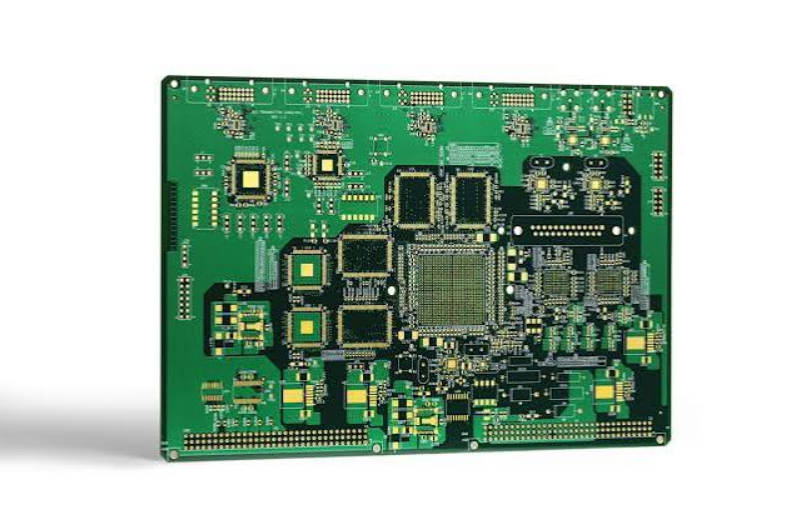
Start Under the BGA, Not in the Stackup Table
The correct HDI structure is the least complex stackup that can route the required components while preserving:
- usable solder-pad dimensions;
- practical trace and space rules;
- adequate reference planes;
- acceptable via aspect ratios;
- signal-integrity margins;
- fabrication yield;
- thermal reliability.
BGA pitch alone does not determine the answer. The escape problem also depends on:
- total pin count;
- power and ground distribution;
- number of differential pairs;
- signal-bank arrangement;
- permitted via-in-pad structures;
- available routing layers;
- board size;
- trace-width requirements.
IPC-published BGA breakout work identifies layer stackup, via models, design rules and signal integrity as the main variables controlling breakout feasibility. It also warns that using a borderline via structure may force smaller features and clearances, reducing fabrication yield and potentially increasing crosstalk.
Historical design guidance also shows that high-pin-count packages below 1 mm pitch are strong drivers for HDI adoption. Modern packages can be considerably denser, but the principle remains valid: as pitch and available escape space decrease, laser microvias become increasingly important.
The stackup should be selected after a preliminary BGA escape study identifies how many independent routing layers must be reached from beneath the package.
Read the Two Stackup Names Correctly
What Is a 2+N+2 HDI Stackup?
The notation describes:
- two sequential buildup layers on the top;
- an N-layer conventionally laminated core;
- two sequential buildup layers on the bottom.
For example, an eight-layer 2+4+2 structure contains two HDI buildup layers above a four-layer core and two below it.
The outer buildup layers commonly use laser-drilled microvias. Connections into or through the central core may use buried mechanical vias, plated through-holes or compound structures combining microvias with buried vias.
Mars-PCB describes 2+N+2 as two high-density outer layers on each side surrounding a conventional inner-layer core. This structure provides more routing headroom than 1+N+1 while retaining a defined core and buildup architecture. (Mars)
What Is Any-Layer HDI?
Any-Layer HDI is commonly referred to as ELIC. Instead of limiting laser microvias to selected outer buildup layers, each layer can participate in the buildup interconnection structure.
The phrase “any layer” does not normally mean one laser via physically drills through any arbitrary number of layers. Individual laser microvias still connect controlled layer spans, commonly between adjacent buildup layers. By filling and stacking those vias, designers can create a conductive path between different layers without relying on one large through-hole.
Commercial ELIC production combines vertically stacked, copper-filled microvias with high-accuracy laser drilling, plating, imaging and registration.
The Structural Difference
| Question | 2+N+2 HDI | Any-Layer HDI / ELIC |
| Where are laser microvias available? | Primarily within two buildup layers on each side | Throughout the multilayer buildup structure |
| Is there a conventional central core? | Yes | May use a coreless or all-buildup-style architecture, depending on design |
| How are deep layers reached? | Microvia plus buried or through-via combinations | Stacked copper-filled microvias across successive layers |
| Routing freedom | High near the outer surfaces | High throughout the board |
| Sequential processing | Multiple buildup cycles | Generally more extensive layer-by-layer buildup |
| Dependence on stacked microvias | Moderate and design-dependent | Usually high |
| Process complexity | High | Very high |
| Cost and yield risk | Lower than equivalent ELIC in many projects | Higher due to additional precision processes |
| Best fit | Dense boards with predictable outer-layer breakout | Extremely dense boards requiring unrestricted layer access |
Test 1: How Many Escape Layers Does the Package Need?
The first practical question is whether two buildup layers on each side provide enough breakout capacity.
A typical 2+N+2 design may route:
- the outer BGA rows on the surface;
- additional rows through the first microvia transition;
- deeper rows through a second buildup transition;
- remaining groups through a buried-via connection into the core.
This can provide substantial routing density without requiring laser microvias on every layer.
When 2+N+2 Is Often Enough
A 2+N+2 structure deserves priority when:
- the BGA escape can be divided cleanly among two buildup layers;
- the central core provides enough additional routing layers;
- only selected signals need access to deep layers;
- buried-via locations do not block critical channels;
- board thickness permits a practical core structure;
- the product does not require extreme miniaturization.
This is common in advanced industrial controls, networking equipment, computing modules and telecommunications hardware where density is high but layer access remains structured.
When the Escape Pattern Starts Fighting the Stackup
Any-Layer becomes more relevant when the layout repeatedly encounters problems such as:
- too many signals competing for the same two escape layers;
- buried-via fields blocking routing channels;
- long horizontal detours before legal layer changes are available;
- differential pairs becoming separated by the via strategy;
- excessive signal-layer count added only to complete the breakout;
- power and ground pins preventing a repeatable fanout pattern;
- multiple fine-pitch packages competing for the same routing resources.
In this situation, adding another conventional signal layer may not solve the real problem. The obstacle may be access to that layer rather than the amount of copper available on it.
Test 2: Does the Layout Need Layer Freedom or Only More Layers?
This distinction is central to the decision.
A designer may conclude that the board needs more routing layers when the actual problem is that signals cannot reach the existing layers efficiently.
What Any-Layer Changes
With ELIC, a signal can transition through successive copper-filled microvias at locations selected for the route rather than being forced toward a buried-via field.
This can provide:
- more direct BGA escape;
- fewer routing detours;
- shorter connections;
- smaller via footprints;
- reduced obstruction on inner layers;
- greater flexibility for differential-pair transitions;
- more options for power and ground distribution.
Commercial Any-Layer processes have been developed specifically to support vertically stacked, copper-filled microvias and very fine-pitch packages.
What Any-Layer Does Not Automatically Fix
ELIC does not automatically solve:
- poor component placement;
- inadequate signal-reference planning;
- unrealistic trace and space rules;
- insufficient power-plane copper;
- excessive crosstalk;
- thermal concentration;
- an inefficient BGA pin assignment.
A poorly planned layout can still consume excessive layers even when every layer is accessible.
Any-Layer provides freedom to change layers; it does not remove the need to allocate those layers deliberately.
Test 3: How Many Microvias Must Be Stacked?
This question separates routing convenience from reliability risk.
A single laser microvia connecting adjacent layers is relatively simple. Stacking several filled microvias vertically creates a compound interconnect with more copper-to-copper interfaces.
IPC has reported industry concerns about latent stacked-microvia failures, including failures that appeared after reflow, environmental testing or field deployment despite passing conventional bare-board inspection. IPC linked many reported failures to the interface between the microvia target pad and the subsequent copper fill.
Why the Interface Matters
A vertically stacked structure may contain:
- a copper-filled lower microvia;
- a plated capture surface;
- another laser-drilled microvia above it;
- an additional copper-fill and capping process.
Thermal expansion places stress on these interfaces during lamination, assembly reflow and product operation.
Studies of compound interconnects have documented more possible failure modes in stacked configurations than in individual or staggered microvias. Some testing has also found staggered structures to be more robust than directly stacked structures under the tested conditions.
This does not mean all stacked microvias are unreliable. It means their reliability depends strongly on:
- microvia geometry;
- aspect ratio;
- target-pad preparation;
- copper-fill quality;
- plating stress;
- material selection;
- number of stacked levels;
- lamination history;
- thermal qualification.
Production processes specifically developed for Any-Layer technology emphasize high-quality copper-to-copper interconnection because delamination and inner-layer interconnect defects directly affect yield and reliability.
The Reliability Choice Is Not Simply 2+N+2 Good, ELIC Bad
Both structures can be reliable when the design and process are qualified.
A 2+N+2 design can also contain risky compound structures if it uses:
- two stacked microvias over a buried via;
- poorly filled via-in-pad features;
- aggressive microvia aspect ratios;
- weak target-pad interfaces;
- incompatible materials;
- excessive thermal processing.
Conversely, an established ELIC production line can manufacture large volumes of stacked microvias when its drilling, copper filling, planarization and registration processes are mature. (Multek)
Relative Reliability Exposure
| Interconnect Structure | Relative Design Simplicity | Main Reliability Concern |
| Single-level microvia | Highest | Corner or target-pad plating quality |
| Staggered microvias | High | Additional routing area and offset requirements |
| Two-level stacked microvia | Moderate | Copper-to-copper interface integrity |
| Microvia stacked on buried via | Moderate to low | Multiple material and plating interfaces |
| Multi-level stacked microvias | Lowest | Accumulated interface and thermal-stress risk |
| Full Any-Layer vertical stack | Application-dependent | Process maturity and performance-based qualification |
The table is directional. Actual reliability must be demonstrated using the selected material, design and supplier process.
Test 4: How Much Sequential Lamination Can the Project Support?
HDI boards are built through repeated imaging, lamination, laser drilling, metallization, copper filling and planarization operations.
In a 2+N+2 process, the conventional inner core is produced first. Buildup layers are then added sequentially to each side.
An ELIC structure extends fine-feature and microvia processing through a larger portion of the complete layer stack. This increases the number of opportunities for:
- registration error;
- dielectric-thickness variation;
- plating nonuniformity;
- copper-fill defects;
- panel distortion;
- yield loss.
Any-Layer production therefore depends on mature laser drilling, copper plating, direct imaging and high-accuracy registration.
What This Means Commercially
Any-Layer HDI usually affects:
- material utilization;
- process cycle time;
- tooling;
- inspection;
- electrical testing;
- reliability-coupon requirements;
- prototype lead time;
- minimum economical volume.
A quotation based only on layer count will not capture the difference. Two 10-layer boards can have very different costs if one is 2+N+2 and the other uses stacked microvias across nearly every layer.
Routing, Reliability and Cost Comparison
| Selection Factor | 2+N+2 HDI | Any-Layer HDI |
| BGA escape flexibility | High | Very high |
| Access to central layers | Restricted by defined via architecture | Flexible through stacked microvias |
| Inner-layer obstruction | Buried vias may consume routing area | Smaller microvia footprints preserve more area |
| Ability to reduce board size | High | Very high |
| Ability to reduce layer count | Moderate to high | Potentially high, depending on layout |
| Differential-pair layer transitions | Must follow available via structures | More transition locations available |
| Microvia stack height | Usually limited | Can be extensive |
| Reliability qualification effort | High | Higher |
| Sequential processing | Significant | More extensive |
| Prototype cost | High | Very high |
| Volume-production risk | Manageable with qualified HDI process | Highly dependent on ELIC process maturity |
| Design flexibility after placement | Moderate | High |
| Recommended default | Yes, when routing is feasible | Only when density or access justifies it |
Select by Product Type
Dense Computing or Networking Board
Start with 2+N+2.
Large processors and FPGAs may require HDI escape, but the board often has enough area and inner routing layers to use a structured core-and-buildup design.
Move toward Any-Layer only when:
- several dense packages compete for space;
- buried-via fields create routing barriers;
- layer count is increasing without solving the escape;
- the mechanical envelope cannot expand.
Smartphone, Wearable or Miniature Module
Any-Layer may be justified earlier.
These products often combine:
- very small board area;
- several fine-pitch packages;
- strict thickness limits;
- high interconnect density;
- short product-routing distances.
Commercial ELIC processes were developed for thin, high-density products such as smartphones, computing modules, wearables and compact IoT devices.
Automotive Control or Sensor Module
Do not select only by density.
Automotive products may need compact routing but also face thermal cycling and long service-life expectations. A 2+N+2 structure with fewer stacked interfaces may be preferable when it meets the layout requirement.
If Any-Layer is necessary, the RFQ should include performance-based thermal testing and supplier-specific reliability evidence.
Medical or Aerospace Electronics
Begin with the lowest-complexity structure that meets the mechanical envelope.
The board may require high density, but field reliability and traceability can outweigh a modest reduction in area. Compound microvia structures should be supported by appropriate test coupons and qualification rather than visual inspection alone.
Camera, Optical or Sensor Module
Any-Layer may offer meaningful size reduction where multiple small packages, image sensors and high-speed interfaces occupy a confined footprint.
The decision still depends on whether the module needs access to every layer or whether two buildup layers already provide enough breakout capacity.
A Practical Selection Worksheet
Answer these questions before fixing the stackup.
1. Can every BGA be escaped with two buildup layers?
If yes, retain 2+N+2 as the baseline.
2. Are buried vias blocking important inner-layer channels?
If yes, compare the routing benefit of ELIC with alternative buried-via placement.
3. Is the layer count increasing because of routing volume or poor layer access?
More routing volume may require more layers. Poor access may justify Any-Layer.
4. How many vertically stacked microvia levels are required?
Do not specify a complete layer-to-layer stack before confirming supplier reliability data.
5. Can some microvias be staggered?
Staggered structures use more lateral space but can reduce dependence on directly stacked interfaces.
6. What thermal profile will the board experience?
Include assembly reflow, rework, environmental testing and field temperature cycling.
7. Is the board-area reduction commercially valuable?
Any-Layer may be reasonable when it enables a smaller product, removes another board or supports a critical package.
8. Is the supplier’s ELIC process already in volume production?
A prototype capability does not automatically demonstrate stable high-volume yield.
Do Not Freeze the BGA Footprint Before DFM
Via-in-pad is frequently required for fine-pitch BGA escape. The finished assembly pad depends on:
- laser-drill diameter;
- capture-pad diameter;
- dielectric thickness;
- copper-fill process;
- cap-plating thickness;
- planarization;
- solder-mask definition.
Microvia geometry must remain within practical depth-to-diameter limits. Industry definitions commonly treat a microvia as a blind structure with an aspect ratio no greater than 1:1 and a maximum depth of 0.25 mm, while many fabricators prefer a more conservative ratio for plating and filling.
Changing the buildup dielectric after layout may therefore invalidate:
- the laser-via geometry;
- the pad size;
- breakout clearance;
- impedance calculations;
- final board thickness.
An early HDI stackup and BGA breakout review should be completed before the footprint, via library and layer transitions are locked.
What to Put in the HDI Fabrication Package
Provide more than a generic note saying “Any-Layer required.”
The fabrication package should include:
- Proposed stackup;
- Buildup sequence;
- Core and buildup materials;
- Finished board thickness;
- Laser-microvia diameter;
- Microvia target and capture pads;
- Dielectric thickness for each microvia;
- Stacked and staggered via map;
- Via-in-pad filling and capping requirements;
- Buried mechanical via structure;
- Controlled-impedance requirements;
- Copper thickness by layer;
- BGA pitch and component information;
- Assembly reflow profile;
- Reliability class and test expectations;
- Prototype and production quantities.
For an ELIC board, also identify:
- maximum microvia stack height;
- which vertical stacks carry critical signals;
- whether a stack terminates on another microvia or buried via;
- permitted via offsets;
- performance-based coupon requirements;
- material and process substitutions requiring approval.
How to Qualify an HDI and ELIC Manufacturer
A supplier evaluation should examine the complete interconnect process.
Ask:
- Which 1+N+1, 2+N+2 and Any-Layer structures are in regular production?
- What laser-via diameters and dielectric depths are routinely controlled?
- How are microvias copper filled and planarized?
- How is copper-to-copper interfacial quality controlled?
- How many stacked levels are qualified for the proposed material?
- Which structures require staggered rather than stacked vias?
- How is sequential-lamination registration measured?
- Are coupons placed on the same production panel?
- Is thermal testing based only on microsections or on continuous resistance monitoring?
- Can the same buildup material and process be maintained from prototype to volume production?
IPC has warned that traditional thermally stressed microsections and optical inspection alone may not detect latent microvia-to-target failures. Performance-based acceptance using resistance-monitoring coupons can provide stronger evidence of interconnect integrity.
Mars-PCB lists 1+N+1, 2+N+2, higher-order sequential buildup and Any-Layer ELIC among its HDI stackup options. A project-specific HDI and ELIC PCB manufacturing review should still confirm the exact material, microvia stack and reliability requirements before quotation. (Mars)
Common Selection Mistakes
Choosing Any-Layer Before Attempting a 2+N+2 Escape
This can add unnecessary cost and qualification work when a simpler structure already satisfies the routing requirement.
Selecting 2+N+2 Only Because It Is Cheaper
If the layout requires excessive layers, narrow traces or long detours, the cheaper stackup may create higher system cost or lower fabrication yield.
Assuming “Any-Layer” Means Unlimited Via Placement
Laser-via depth, aspect ratio, capture-pad size and registration still constrain the design.
Building Long Vertical Microvia Stacks by Default
Every added level introduces another interface that must survive fabrication, assembly and field temperatures.
Treating Electrical Continuity as Reliability Proof
A microvia may pass room-temperature electrical test and fail after reflow or thermal cycling.
Ignoring Buildup Material Properties
Thin buildup dielectrics affect impedance, laser drilling, resin flow, copper adhesion and Z-axis expansion.
Quoting the Board Without BGA Information
The supplier cannot properly assess escape feasibility without the package pitch, pad geometry and pin-field structure.
Using the Same Via Library for Different Fabricators
Laser diameter, dielectric thickness, pad size and copper-fill capability are process-specific.
FAQ
What does 2+N+2 mean in an HDI PCB?
It means the board has two sequentially laminated buildup layers on each side of an N-layer conventional core. Laser microvias connect the buildup layers, while buried or through-vias may connect the central core.
What is Any-Layer HDI PCB?
Any-Layer HDI, also called ELIC, uses copper-filled laser microvias throughout the multilayer structure. Stacked microvias allow signals to access different layers without relying on large through-holes.
Is Any-Layer HDI better than 2+N+2?
Any-Layer provides greater routing freedom and density, but it is not automatically better. A 2+N+2 stackup is usually more economical and may offer a simpler reliability path when it satisfies the BGA breakout.
Which HDI stackup is suitable for a 0.5 mm BGA?
Both may be possible. The correct choice depends on pin count, ball pattern, via-in-pad geometry, number of escape layers and manufacturer design rules. A preliminary breakout study is required.
Does Any-Layer HDI require stacked microvias?
Most ELIC structures rely heavily on vertically stacked, copper-filled microvias to connect successive layers. The exact stack height and location should be minimized where practical.
Are stacked microvias reliable?
They can be reliable when geometry, copper fill, target-pad preparation and plating are tightly controlled. Compound stacks require more qualification because each interface adds a potential failure location.
Are staggered microvias more reliable than stacked microvias?
Staggered microvias avoid placing each via directly over the previous one and can reduce interface stress. They require more lateral board space, so the choice depends on both density and reliability requirements.
Is Any-Layer HDI always more expensive?
It is generally more expensive because it requires more extensive sequential processing, laser drilling, copper filling, planarization, registration control and inspection. The total product cost may still be justified if it reduces board size or layer count.
Can Any-Layer HDI improve signal integrity?
It can shorten routes and provide more direct layer transitions. Signal integrity still depends on reference-plane continuity, impedance geometry, crosstalk and transition design.
How should microvia reliability be tested?
Testing may include resistance-monitoring coupons subjected to reflow simulation, thermal stress or thermal cycling. Conventional microsections alone may not reveal latent microvia-interface failures.
Conclusion
The Any-Layer HDI vs 2+N+2 decision should be made from the BGA escape outward.
A 2+N+2 stackup provides substantial routing density and should normally remain the first option when two buildup layers on each side provide sufficient access to the inner routing structure.
Any-Layer HDI becomes valuable when fixed buildup zones and buried-via fields prevent the board from reaching its size, layer-count or interconnect-density targets.
Choose 2+N+2 when structured layer access is sufficient; choose Any-Layer when unrestricted layer access creates a measurable product or routing advantage.
Whichever structure is selected, define the microvia geometry, buildup material, stacked-via locations and performance-based reliability tests before releasing the layout.
For a feasibility review, submit the BGA files, preliminary layer count, board thickness and via map through the Mars-PCB website so the breakout strategy and manufacturing sequence can be assessed together.