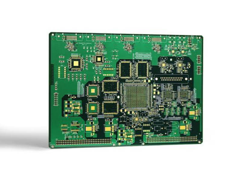
CXL 4.0 PCB design operates on the PCIe 7.0 physical layer at 128 GT/s. Because PAM4 signaling at this data rate has a 32 GHz Nyquist frequency, PCB loss, copper roughness, via stubs, connectors and ordinary fabrication variation become critical parts of the system architecture.
The move to 128 GT/s does not create one mandatory “CXL 4.0 material,” but it does require every laminate and stackup decision to be justified against the complete channel-loss budget.
The CXL 4.0 specification was released in November 2025. It doubles the maximum link rate from 64 GT/s to 128 GT/s, retains PAM4 signaling, introduces native x2 support and Bundled Ports, and allows up to four retimers for extended reach. CXL 4.0 also continues to support Type 1, Type 2 and Type 3 devices, memory pooling and CXL fabric capabilities established by earlier generations.
For AI servers, memory expanders and accelerator platforms, this is not simply another speed increase. It changes how engineers must plan routing density, signal-layer allocation, material loss, reference planes, layer transitions and production validation.
The 128 GT/s Design Brief
CXL 4.0 builds on the PCIe 7.0 PHY. It uses PAM4 signaling at 128 GT/s and doubles the Nyquist frequency from the 16 GHz used at 64 GT/s to 32 GHz. Its physical-layer design therefore inherits the major signal-integrity challenges associated with PCIe 7.0 channels.
| CXL 4.0 Characteristic | PCB Consequence |
| 128 GT/s link rate | Greater insertion loss and tighter channel margin |
| 32 GHz Nyquist frequency | Increased sensitivity to dielectric loss and copper roughness |
| PAM4 signaling | Three eyes with less vertical margin than NRZ |
| PCIe 7.0 PHY | PCIe 7.0 channel and component performance become directly relevant |
| Native x2 link support | More flexible fan-out but potentially greater routing density |
| Bundled Ports | Multiple physical links may need coordinated stackup and routing resources |
| Up to four retimers | Longer architectures are possible, but each electrical segment still requires validation |
| CXL memory and coherency traffic | Stable latency and link reliability remain important at the system level |
A 128 GT/s channel must be planned as a sequence of interacting structures:
- processor or host package;
- BGA escape;
- motherboard routing;
- AC-coupling capacitor;
- vias and layer transitions;
- card-edge, board-to-board or cable connector;
- riser, backplane or add-in card;
- retimer, switch or memory device package.
A differential pair that appears short on the layout may still consume substantial channel margin when packages, connectors and transitions are included.
The Material Decision Is Really a Loss Allocation Decision
The correct starting point is not a laminate brand or material grade. It is the maximum loss that the PCB portion of the link can consume after the package, connector and device contributions are considered.
Public PCIe 7.0 technical guidance identifies an approximate die-pad-to-die-pad loss budget of 36 dB at 32 GHz. In the example allocation, the root package consumes approximately 9 dB and the non-root package approximately 4 dB, leaving around 23 dB for the remaining interconnect. The applicable allocation still depends on the topology, component models and compliance requirements. (PCI-SIG)
A laminate should be selected from the remaining PCB loss allowance, not from the protocol name printed on a data sheet.
The available PCB budget may need to cover:
- host-board routing;
- breakout and neck-down regions;
- layer-transition vias;
- AC-coupling capacitor pads;
- connector launches;
- add-in-card routing;
- retimer-board routing;
- manufacturing and modelling margin.
Two CXL 4.0 systems can therefore require different material classes. A short host-to-device connection may have more material flexibility than a server motherboard connected through a riser, backplane or add-in card.
A Practical Material Evaluation Matrix
| Property | Why It Matters at 32 GHz | What the Engineering Team Should Request |
| Dissipation factor, Df | Influences frequency-dependent dielectric loss | Df at relevant frequencies and the test method used |
| Dielectric constant, Dk | Affects impedance, delay and routing dimensions | Frequency-dependent Dk and resin-content information |
| Copper profile | Influences conductor loss as surface current follows copper topography | Copper roughness classification and available foil options |
| Glass style | Can contribute to local impedance variation and intra-pair skew | Proposed core and prepreg glass constructions |
| Resin content | Changes effective electrical properties and pressed thickness | Actual production constructions rather than generic data |
| Thickness tolerance | Directly affects impedance and coupling | Finished dielectric and overall board tolerances |
| Thermal reliability | Must support assembly and long-term server operation | Applicable thermal and reliability test information |
| Material availability | Determines whether prototypes can be reproduced in production | Approved material list and substitution policy |
Why Nominal Df Is Not Enough
A low nominal Df can be useful, but it is not a complete predictor of channel performance.
Published Df values may differ because of:
- test frequency;
- test method;
- resin percentage;
- sample thickness;
- copper treatment;
- moisture condition;
- material anisotropy.
The simulation model should correspond to the actual pressed stackup as closely as possible. Using a single generic Dk and Df value for every frequency can create an optimistic loss estimate.
For long server channels, official PCIe 7.0 guidance indicates that PCB loss around or below 1 dB per inch at 32 GHz may be needed. It also notes that very-low-loss materials combined with minimal copper surface roughness can help reach this level. This is a planning reference rather than a universal acceptance limit for every CXL 4.0 topology. (PCI-SIG)
Copper Roughness Can Change the Result of the Same Laminate
At 32 GHz, conductor loss is strongly affected by the surface over which current flows. A rough copper profile increases the effective current path and may raise attenuation.
This means two boards using the same resin system can produce different high-frequency results when they use different copper foils or surface treatments.
The stackup request should identify:
- low-profile or very-low-profile copper where required;
- copper type on cores and foils;
- finished copper thickness;
- whether the roughness model used in simulation represents the production foil;
- whether the fabricator may substitute another copper treatment.
Specifying an ultra-low-loss dielectric without controlling copper roughness can leave a major source of 32 GHz loss unmanaged.
Lower-profile copper must still meet adhesion and reliability requirements. The objective is not to request the smoothest copper in isolation, but to qualify a laminate-and-copper system that the fabricator can process consistently.
Build the CXL 4.0 Stackup from the Signal Layers Out
There is no universal 12-layer, 16-layer or 20-layer CXL 4.0 stackup. Layer count is a result of routing density, breakout strategy, power architecture, link count, mechanical thickness and loss targets.
A more reliable method is to define each critical signal layer together with its nearest reference plane before arranging the remaining power and low-speed layers.
Step 1: Assign the Critical CXL Layers
Place the most demanding CXL links on layers that provide:
- continuous reference planes;
- short via transitions;
- controlled dielectric thickness;
- practical trace width and spacing;
- low-loss routing without unnecessary serpentine sections;
- sufficient separation from noisy signal groups.
For dense server boards, placing all high-speed pairs on only one or two layers can create congestion, excessive layer changes and poor breakout geometry. Adding another well-referenced signal layer may produce a better channel than forcing longer routes onto fewer layers.
Step 2: Choose Stripline or Microstrip Deliberately
| Routing Structure | Potential Advantages | Main Risks |
| Surface microstrip | Easy probing, fewer layer transitions and potentially shorter escape | Greater exposure to environmental variation and solder-mask effects |
| Embedded microstrip | Can support controlled surface-adjacent routing | Requires careful treatment of nearby dielectric and mask |
| Symmetric stripline | Strong field containment and stable reference planes | More dielectric and conductor loss over equivalent distance |
| Offset stripline | May improve routing flexibility and coupling control | Requires accurate modelling of asymmetric dielectric spacing |
Stripline is commonly used for long internal server-board routing because it provides strong reference-plane control and reduced external coupling. However, the additional dielectric interaction can increase loss relative to some surface structures.
The decision must come from channel simulation, not a rule that every CXL lane should use the same routing structure.
Step 3: Control Reference-Plane Continuity
A differential pair does not eliminate the need for a stable return path. Real channels contain common-mode energy caused by geometry imbalance, package transitions, connectors and vias.
Critical CXL pairs should avoid:
- crossing reference-plane splits;
- passing over anti-pad fields that excessively interrupt return current;
- switching between unrelated reference voltages without transition planning;
- routing close to plane edges;
- sharing congested return paths with noisy power-conversion regions.
When a pair changes reference planes, nearby ground stitching vias can help provide a controlled transition path. Their number, spacing and placement should be included in the transition model.
Stackup Parameters That Should Not Be Finalized Independently
Trace Width and Spacing
At 128 GT/s, the narrowest routable trace is not automatically the correct trace.
Very narrow conductors may:
- increase conductor loss;
- become more sensitive to etching variation;
- require smaller spacing to maintain differential impedance;
- complicate volume-production control.
Wider traces may reduce conductor loss but require a different dielectric thickness or larger routing channels. The final geometry should balance loss, impedance, density and fabrication tolerance.
Differential Impedance
The target impedance must be derived from the relevant CXL and PCIe implementation requirements. The fabrication package should also specify:
- finished impedance rather than nominal artwork impedance;
- permitted tolerance;
- layer-specific structures;
- coupon requirements;
- whether solder mask is present;
- measurement and reporting method.
Impedance control alone does not verify a 128 GT/s channel. A board can pass a time-domain impedance coupon while still having excessive insertion loss or resonant discontinuities.
Glass-Weave Interaction
Because the two conductors of a differential pair may encounter different proportions of glass and resin, local propagation velocity can differ. At high frequencies, this may create intra-pair skew.
Possible mitigation methods include:
- selecting tighter or more uniform glass styles;
- routing pairs at a slight angle relative to the weave;
- using wider traces that average a larger material area;
- coordinating resin-rich constructions with the fabricator;
- evaluating skew through simulation and test coupons.
These measures should be considered together with material availability and manufacturability.
Layer Transitions May Determine Whether the Stackup Works
The best low-loss signal layer can still produce a poor channel if the pair reaches it through an uncontrolled via structure.
A plated through-hole transition introduces:
- barrel inductance;
- pad capacitance;
- anti-pad discontinuity;
- coupling between adjacent vias;
- return-path disturbance;
- an unused stub when the signal exits before the final layer.
At 32 GHz, the unused barrel can form a resonant structure within or close to the operating band.
Comparing Transition Options
| Transition Method | Potential Benefit | Manufacturing Trade-Off |
| Through-via without backdrill | Lowest process complexity | Unused stub may create unacceptable resonance |
| Backdrilled through-via | Removes much of the unused barrel | Requires depth control and measurable residual-stub limits |
| Blind via | Avoids a long through-hole stub | Adds HDI processing and lamination complexity |
| Buried via | Supports internal layer connections | Increases sequential-build and registration requirements |
| Microvia transition | Compact breakout for dense packages | Requires careful reliability and stacking evaluation |
| Layer assignment that minimizes transition depth | Reduces stub without another process | May constrain routing and stackup organization |
For CXL 4.0, backdrilling should be specified through a residual-stub requirement, not through a vague note requesting “backdrill high-speed vias.”
The manufacturing drawing should identify:
- drilling side;
- target layer;
- backdrill diameter;
- maximum permitted residual stub;
- depth tolerance;
- whether non-functional pads should be removed;
- inspection or verification method.
A supplier should confirm that the requested depth is compatible with the finished dielectric thicknesses and its registration capability.
Bundled Ports Create a Routing-Density Problem as Well as a Bandwidth Opportunity
CXL 4.0 introduces Bundled Ports, which can aggregate multiple physical device ports into a single logical connection. It also introduces native x2 width support for increased platform fan-out.
These features affect PCB planning because a platform may need:
- more independent high-speed links;
- coordinated escape from multiple host or device ports;
- consistent lane-to-lane performance;
- additional connector or retimer locations;
- more reference-plane resources;
- greater separation between high-speed lane groups;
- additional power delivery for switches or retimers.
The stackup should therefore be evaluated at the platform level. Designing one compliant pair does not prove that dozens of adjacent pairs can be routed with acceptable crosstalk and manufacturing margin.
Three Architecture Paths for a 128 GT/s CXL Channel
| Architecture | When It May Be Appropriate | PCB Design Priority |
| Direct host-to-device connection | Short motherboard or local accelerator connection | Minimize transition count and total routed distance |
| Retimer-segmented connection | Longer path, connector-rich topology or modular server design | Treat each retimer segment as a separately valid channel |
| PCB plus cable or fly-over connection | Board reach is limited by PCB loss or routing congestion | Optimize board-to-cable launches, skew, reflections and crosstalk |
CXL 4.0 supports up to four retimers for increased channel reach, but this does not make PCB loss irrelevant. Each segment between devices or retimers must still meet its electrical requirements.
A retimer decision should account for:
- channel loss;
- connector count;
- system modularity;
- power consumption;
- thermal placement;
- clocking architecture;
- device availability;
- latency requirements;
- validation complexity.
It is usually more efficient to make this decision during system architecture development than to add a retimer after the board layout has already been completed.
Translate the Simulation Stackup into a Production Stackup
A simulation model describes dimensions and electrical properties. A fabrication drawing must describe how those values will be achieved and verified.
Before releasing the board, the engineering team and high-speed PCB manufacturing supplier should align on the following items.
Material Controls
- exact laminate family or approved alternatives;
- core and prepreg construction;
- glass styles and resin content;
- copper profile;
- permitted material substitution;
- frequency-dependent electrical data used for modelling.
Geometry Controls
- finished dielectric thickness;
- finished trace width and spacing;
- copper thickness;
- impedance tolerance;
- registration tolerance;
- via and anti-pad dimensions;
- backdrill depth and residual stub.
Validation Controls
- impedance coupons;
- insertion-loss or channel coupons where needed;
- TDR reporting;
- backdrill inspection;
- stackup cross-section;
- material certificates or lot traceability where required;
- first-article and production reporting expectations.
An early CXL PCB stackup review can identify conflicts between the simulated geometry and the fabricator’s practical line-width compensation, material inventory or pressing tolerances.
Why Nominal Simulation Is Not Sufficient
A nominal model assumes that every value is manufactured exactly as specified. Production includes variation in:
- trace width;
- copper thickness;
- dielectric thickness;
- Dk and Df;
- resin distribution;
- layer registration;
- drill position;
- plating thickness;
- backdrill depth;
- connector mounting.
The channel should therefore be evaluated across realistic process corners.
| Simulation Level | What It Shows | What It May Miss |
| Nominal transmission-line model | Initial impedance and loss estimate | Complex via and connector fields |
| Three-dimensional transition model | Via, connector and capacitor-pad behavior | Production distribution |
| Statistical or corner analysis | Sensitivity to tolerances | Incorrect material assumptions |
| Fabricated coupon correlation | Difference between model and production | Full system behavior if coupon is not representative |
| Complete-channel simulation | End-to-end performance | Errors in package or connector models |
A practical objective is not merely to obtain one passing nominal result. It is to create enough margin that normal fabrication variation does not push a significant number of production boards outside the intended channel performance.
Common CXL 4.0 Stackup Errors
Selecting the Material Before Defining the Topology
A laminate cannot be qualified without knowing the routing length, package contribution, connector count and retimer strategy.
Using Generic Data-Sheet Values in the Final Model
Generic Dk and Df values may not represent the selected resin content, copper profile or test frequency.
Optimizing Impedance While Ignoring Insertion Loss
Changing trace width, spacing and dielectric thickness to hit impedance can unintentionally increase conductor or dielectric loss.
Placing CXL Layers Too Deep in the Board
Deep routing layers may require long via transitions and larger backdrill depths. Layer position should be evaluated together with BGA escape and connector access.
Allowing Reference-Plane Changes Without Stitching Planning
The differential pair may remain visually continuous while its return-current environment changes abruptly.
Defining Backdrill by Target Layer Only
Layer thickness variation can change the remaining stub. The acceptance requirement should address the finished residual stub.
Treating Every Pair as an Independent Channel
Dense CXL links must also be evaluated for lane-to-lane crosstalk, breakout congestion and shared reference-plane effects.
What to Include in a CXL 4.0 PCB RFQ
A technically useful RFQ should contain more than Gerber or ODB++ files.
Provide:
- CXL generation and target link rate;
- device and channel topology;
- preliminary stackup;
- critical pair lengths and layer assignments;
- impedance targets and tolerances;
- insertion-loss objective or material-loss requirement;
- approved material class;
- copper-profile preference;
- via and backdrill drawings;
- connector and package-transition information;
- coupon and reporting requirements;
- prototype quantity and expected production volume.
Ask the supplier to respond with:
- a proposed production stackup;
- actual core and prepreg constructions;
- adjusted finished trace geometry;
- material availability;
- achievable impedance tolerance;
- achievable residual backdrill stub;
- proposed coupon method;
- any deviations from the supplied model.
The purpose of the RFQ is not only to obtain a price. It should expose whether the supplier understands the connection between electrical assumptions and manufacturing controls.
How to Qualify a CXL PCB Manufacturer
A capable supplier does not need to claim that every board will automatically support CXL 4.0. It should be able to explain how the proposed construction will be evaluated.
Review whether the supplier can:
- process appropriate low-loss material systems;
- control low-profile copper constructions;
- collaborate on stackup impedance modelling;
- perform precision backdrilling;
- manufacture fine-pitch BGA transitions;
- provide impedance and loss-related coupons;
- document material substitutions;
- correlate finished geometry with the design model;
- support prototype-to-production stackup consistency.
For a new server or memory-expansion project, Mars-PCB can review the preliminary construction as part of a 128 GT/s high-speed PCB fabrication discussion. The most useful review package includes the topology, loss assumptions, critical transitions and expected production controls.
FAQ
What PCB material is needed for CXL 4.0?
CXL 4.0 does not require one universal laminate. Material selection depends on the 32 GHz loss target, routed length, copper roughness, connectors, packages, vias and retimer architecture. Longer server channels commonly require very-low-loss laminate and low-profile copper.
Is CXL 4.0 based on PCIe 7.0?
Yes. CXL 4.0 uses the PCIe 7.0 physical layer at 128 GT/s. It retains PAM4 signaling and uses a 32 GHz Nyquist frequency.
What is the target impedance for a CXL 4.0 PCB?
The target must follow the applicable CXL and PCIe implementation requirements. Designers should specify finished differential impedance, tolerance, layer structure and coupon method rather than relying only on nominal artwork geometry.
How many layers does a CXL 4.0 server PCB need?
There is no fixed layer count. The required number depends on processor breakout density, lane count, Bundled Ports, power distribution, board thickness, connector topology and the number of low-loss signal layers needed.
Does CXL 4.0 require backdrilling?
Not every CXL 4.0 via must be backdrilled. Backdrilling is appropriate when an unused through-via stub creates excessive reflection or resonance. Blind vias, microvias or different layer assignments may also reduce the stub.
How does copper roughness affect a 128 GT/s PCB?
Rough copper increases the effective current path and can raise conductor loss at high frequencies. The copper profile should therefore be included in material selection, simulation and fabrication documentation.
Can a retimer solve excessive CXL PCB loss?
A retimer can divide a long connection into shorter electrical segments, but each segment must still be designed correctly. It does not remove local reflection, via, connector or crosstalk problems.
Should a CXL 4.0 PCB be tested only for impedance?
No. Controlled impedance is important, but it does not prove acceptable insertion loss or transition performance. Depending on the project, validation may also require loss coupons, TDR, backdrill inspection and correlation with the channel model.
Conclusion
CXL 4.0 doubles the link rate to 128 GT/s while preserving the low-latency, coherent connectivity needed by memory expanders, accelerators and data-center platforms. That bandwidth increase moves the PCB into a regime where material models, copper roughness, reference planes, via stubs and manufacturing tolerances directly affect system feasibility.
The right CXL 4.0 stackup is the construction that meets the complete 32 GHz channel target and can be reproduced consistently in fabrication.
Engineering teams should define the topology and loss allocation first, select materials with production-specific data, build signal layers around stable reference planes, model every critical transition and establish measurable fabrication requirements.
Submitting these requirements early through the Mars-PCB high-speed PCB service allows the stackup, impedance geometry, material availability and backdrill structure to be reviewed before prototype release.