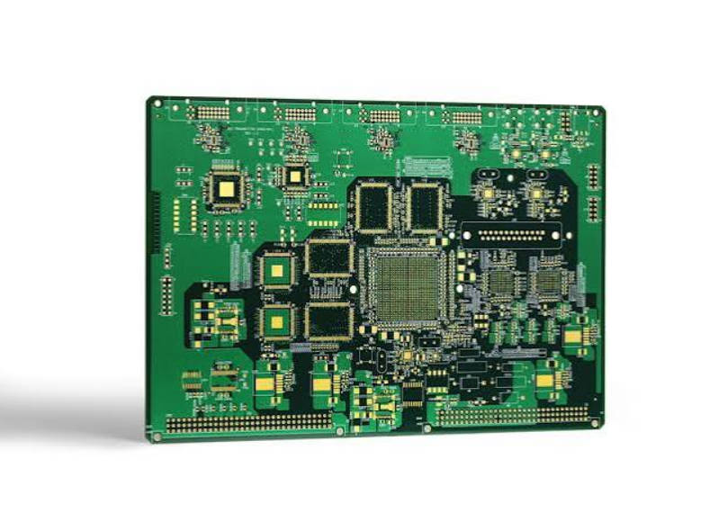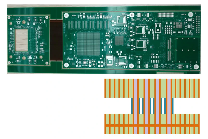
An AI server backplane is not simply a large circuit board. It has to carry high-speed differential pairs across distances that would be trivial on a daughter card, while simultaneously delivering hundreds of amps at low voltage to the compute modules plugged into it. Those two jobs pull the design in opposite directions: signal integrity wants thin dielectrics and tight impedance control, while power delivery wants thick copper and generous plane area. Understanding where those requirements conflict is the core of backplane design. This article covers what changes at backplane scale, how the signal and power sides each behave, and what to confirm with your fabricator before releasing the design.
What Makes a Backplane Different from a Daughter Card
The functional difference is that a backplane is a passive interconnect structure. It carries signals and power between daughter cards — compute modules, switch fabrics, accelerator trays — rather than hosting active components itself. That has several practical consequences.
First, thickness. A backplane often runs between 3 mm and 6 mm or more, compared with 1.6 mm for a typical board. Thickness is driven by mechanical requirements: the board has to support the weight of plugged-in modules, resist bowing under their mass, and keep press-fit connector pins aligned. Mechanically, a thin board spanning a large rack width will flex enough to cause connector mating problems.
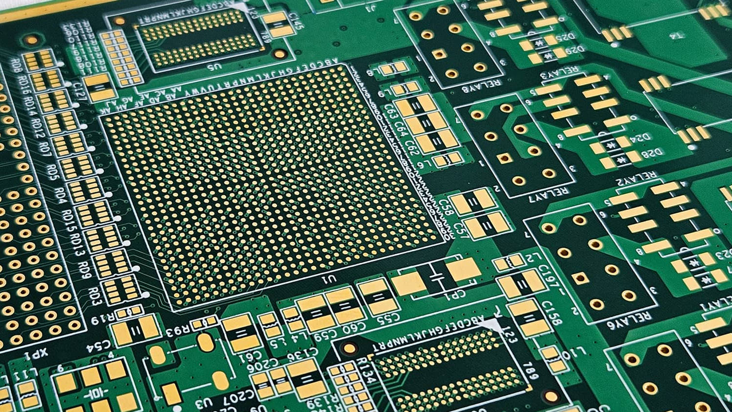
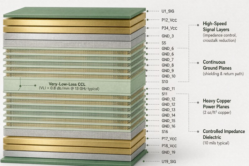
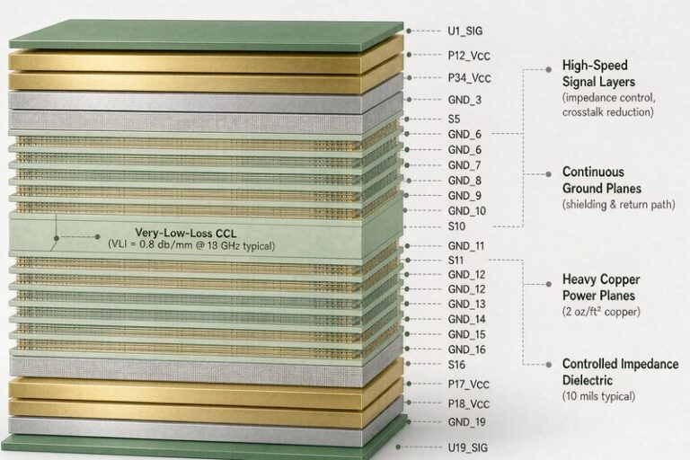
Second, layer count. Because the board carries both a large number of high-speed differential pairs and a substantial power delivery network, layer counts in the 16 to 30 range are common, and some designs go higher. A Multilayer PCB at this scale introduces lamination and registration considerations that do not appear in smaller builds — more lamination cycles, more drill-to-inner-layer registration risk, and a greater chance of warp if the stackup is not balanced.
Third, the via structure. A backplane is dominated by through-hole vias for connectors, and those vias pass through the entire board thickness. A via barrel spanning 5 mm behaves very differently from one spanning 1.6 mm — both electrically, because of the added capacitance and stub length, and mechanically, because of the aspect ratio limit on drilling and plating.
Signal Integrity at Backplane Distances
On a daughter card, a 10 cm trace is unremarkable. On a backplane, a route between two slots can be 50 cm or longer, and every loss mechanism scales with distance. Three effects dominate.
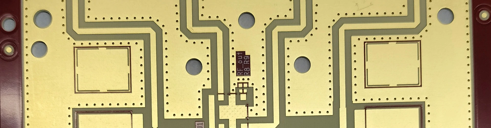
Insertion loss. Dielectric loss and conductor loss both accumulate along the route. At the 112 Gbps PAM4 rates used in current AI fabrics, the loss budget is tight enough that laminate grade and copper foil profile become design decisions rather than purchasing details. This is the point where backplane design overlaps with high-speed PCB practice: the same material and geometry rules apply, but with far less margin.
Via stubs. A press-fit connector pin does not use the full barrel length, so the unused lower portion of the through-hole via acts as a resonant stub. At backplane thicknesses, that stub can be several millimetres long, which puts its resonance well inside the operating band. Back-drilling — removing the unused barrel from the back side — is standard practice on high-speed backplanes for exactly this reason.
Impedance continuity. Every transition — connector footprint, via, layer change — introduces a discontinuity. On a short route these are absorbed; on a long route they accumulate and interact. Holding controlled impedance through the connector region is usually the hardest part of the design, because the connector vendor’s footprint often dictates pad geometry that is not impedance-ideal.

Crosstalk deserves a mention as well. Backplanes are dense by necessity, and long parallel routes have plenty of length in which to couple. Spacing rules, and where necessary ground vias between aggressor and victim pairs, have to be planned at the layout stage rather than retrofitted.
Power Distribution: The Other Half of the Problem
A modern accelerator module can draw well over a kilowatt. Multiply that across a fully populated backplane and the power delivery network has to move hundreds of amps at voltages that may be below 1 V. Ohm’s law is unforgiving at that combination: even a fraction of a milliohm in the distribution path translates into meaningful voltage drop and heat.
The design responses are largely geometric:
- Thicker copper on power planes. Moving from 1 oz to 2 oz or 3 oz copper on the power and ground planes reduces both DC drop and temperature rise. On the power side of an AI backplane, heavy copper is not exotic — it is the baseline.
- More plane layers in parallel. Multiple power planes strapped together with via arrays reduce effective resistance and provide a lower-inductance return path.
- Generous via counts at the connector. Power and ground pins are used in large numbers, and the via field connecting them to the planes needs to be sized accordingly.
- Thermal relief planning. Power dissipated in the planes has to leave the board somehow. In forced-air systems this is manageable; in sealed or high-density systems it becomes a first-order constraint.
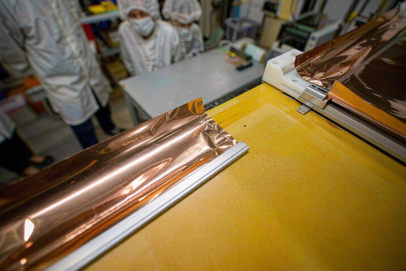
This is where heavy copper PCB capability matters. Plating and etching thick copper on a board that is already 4–6 mm thick is a different process from doing it on a 1.6 mm board, and not every fabricator handles both extremes in the same panel. Etch compensation for thick copper also affects trace geometry, which feeds back into the impedance calculation.
Connectors, Press-Fit and Mechanical Reality
Backplane connectors are typically press-fit rather than soldered. The connector pin is forced into a plated through-hole, and the interference fit makes the electrical and mechanical connection. This has direct implications for the board.
Hole size and plating thickness are tightly toleranced: too little plating and the joint is weak or high-resistance, too much and the pin will not seat or will damage the barrel. Hole tolerance interacts with the finished hole size after plating, so the fabricator needs to know which holes are press-fit and which are not — a detail that is easy to omit from a fabrication drawing and expensive to discover later.
Aspect ratio is the other constraint. Drilling and reliably plating a 0.3 mm hole through a 5 mm board is a roughly 17:1 aspect ratio, which is at or beyond what many shops will guarantee. Design rules that look fine on a thin board may be unmanufacturable on a thick one, so the via specification should be discussed before layout is finalised.
What to Confirm Before Ordering
Backplanes are among the most expensive boards a system contains, and among the slowest to re-spin. A short checklist of items to settle with the fabricator early:
- Maximum board thickness and finished thickness tolerance, including the effect of multiple lamination cycles.
- Whether back-drilling is required, and the remaining stub length that can be held.
- Aspect ratio capability for the smallest via at the finished thickness.
- Press-fit hole tolerances and which holes they apply to.
- Copper weights per layer, and whether heavy copper and fine-line signal layers can coexist in the same stackup.
- Warpage limit after reflow, since a bowed backplane creates connector mating problems.
- Material availability at the required thickness and copper weight — PCB Raw Materials Library selection for thick, high-layer-count builds is narrower than for standard boards, and lead times are longer.
Because most of these constraints are geometric rather than electrical, they are cheapest to resolve during DFM review, before the design is released to tooling. A backplane that is electrically sound but mechanically unmateable is a complete loss, and that failure mode is far more common than a pure signal-integrity failure.
Conclusion
Backplane design is a two-sided problem. The signal side is governed by distance: loss accumulates, via stubs resonate, and impedance discontinuities compound, all of which push toward low-loss laminate, back-drilled vias and controlled impedance through the connector region. The power side is governed by current: hundreds of amps at sub-1 V demand thick copper, parallel planes and large via fields, which push in the opposite geometric direction.
The mechanical layer sits underneath both. Board thickness is set by the need to support modules and keep press-fit pins aligned, and that thickness then drives aspect ratio limits, stub length and drilling capability. In practice, more backplane projects run into trouble on thickness, aspect ratio or hole tolerance than on the electrical design itself.
If you are planning an AI server backplane, share the layer count, thickness, copper weights and connector type, and we can review the stackup and via structure against what is actually manufacturable.
FAQ
How thick is a typical AI server backplane?
Most run between 3 mm and 6 mm, significantly thicker than the 1.6 mm of a standard board. The thickness comes from mechanical requirements — supporting plugged-in modules, resisting bow, and keeping press-fit pins aligned — rather than from electrical need.
Why is back-drilling almost always needed on high-speed backplanes?
A press-fit connector pin does not use the full via barrel, so the unused portion becomes a resonant stub. At backplane thicknesses that stub can be several millimetres long, placing its resonance inside the operating band. Back-drilling removes it.
Can heavy copper and high-speed signal layers coexist in one backplane?
Yes, and this is common — thick copper on the power and ground planes, thinner copper on the signal layers. It requires the fabricator to handle both etch regimes in one panel, and etch compensation on the thick layers has to be accounted for in the impedance calculation.
What usually causes a backplane project to fail?
Mechanical and geometric issues more often than electrical ones: via aspect ratio beyond the fabricator’s capability, press-fit hole tolerances that were not specified, or warpage after lamination that prevents connector mating. These are best resolved during DFM review.