Copper foil thickness sets the floor on how fine a trace you can etch. Standard 1 oz foil is about 35 µm thick, and etching a 50 µm trace through 35 µm of copper produces a visibly trapezoidal cross-section with significant undercut. Drop the starting foil to 12 µm or thinner and the same trace etches with near-vertical walls, because there is far less copper to remove and far less time for lateral etching to occur. That single change is what makes 25 µm line-and-space production practical, and it is why ultra-thin copper foil has become a defining material for high-density interconnect, IC substrate and fine-line mSAP builds. This article explains the mechanism, where ultra-thin foil is genuinely required, and what it costs in handling, current capacity and process risk.
What “Ultra-Thin Copper” Means in Practice
Copper foil for PCB laminates is specified by weight per unit area, and the industry converts that to a nominal thickness:
| Common designation | Nominal thickness | Typical application |
|---|---|---|
| 1 oz | ~35 µm | General boards, power planes, high-current routing |
| 0.5 oz | ~17.5 µm | Signal layers on standard multilayer boards |
| 1/3 oz | ~12 µm | Fine-line routing, HDI core layers |
| 1/4 oz | ~9 µm | Advanced HDI, fine-line circuits |
| Ultra-thin carrier-backed foil | 2–5 µm | mSAP / IC substrate processes |
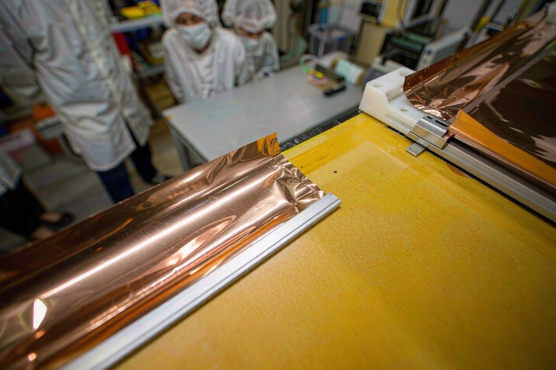
“Ultra-thin” generally starts at 12 µm and below. Below about 5 µm the foil is usually supplied on a carrier — a thicker supporting foil or film that is peeled away after lamination — because free-standing copper that thin cannot be handled without wrinkling or tearing.
It is worth separating two different uses, because they are often conflated. The first is using thin foil as the finished conductor weight on a signal layer. The second is using an extremely thin base foil as a seed layer, then plating the traces up to their final thickness, which is how mSAP works. The first is a straightforward material substitution; the second is a different process flow with different equipment requirements.
Why Foil Thickness Controls Fine-Line Capability
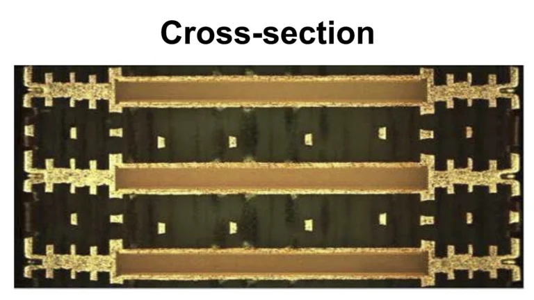
The relationship comes down to etch factor. Wet etching removes copper isotropically — it attacks sideways at the same time as it attacks downward. To etch a trace through a thick foil, the panel stays in the etchant longer, and over that longer time the sideways attack eats further under the resist mask. The result is undercut: the top of the trace is narrower than the base, producing the classic trapezoidal cross-section.
Two practical consequences follow:
- Minimum trace width. With thick foil, a trace narrow enough at the top risks being undercut through entirely at the base. The usable minimum width is therefore tied to how much copper has to be removed.
- Impedance accuracy. A trapezoidal cross-section does not behave like the rectangular one that impedance calculators assume. As traces get finer, the deviation grows, which matters when holding controlled impedance on a fine-line design.
Starting with thinner copper shortens the etch time, reduces undercut, and yields a cross-section much closer to vertical. That is the entire argument for ultra-thin foil: it does not change the copper’s electrical properties, it changes the geometry you can reliably produce.
This matters more the finer the design rules go. At 100 µm line-and-space, standard foil is fine. At 50 µm it starts to bite. Below 30 µm, thin foil stops being an optimisation and becomes a requirement.
Where Ultra-Thin Foil Is Actually Required
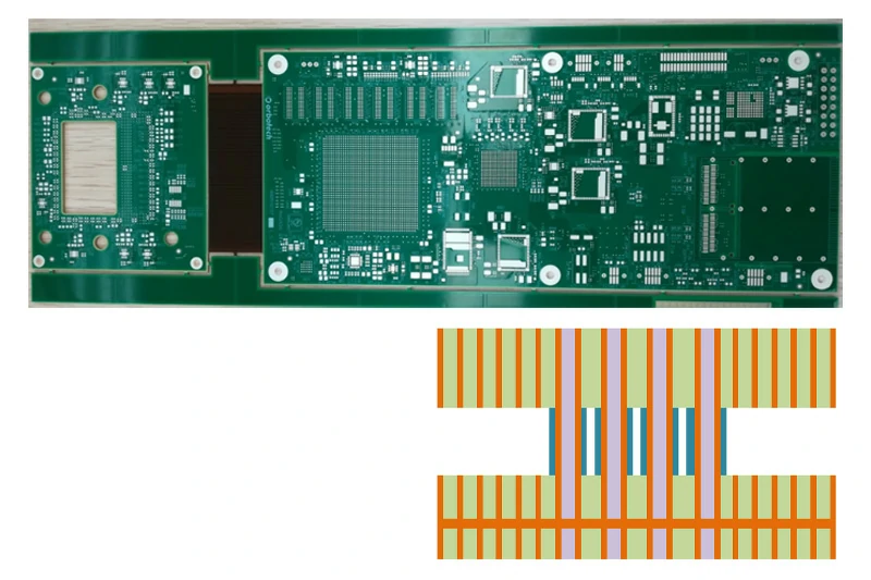
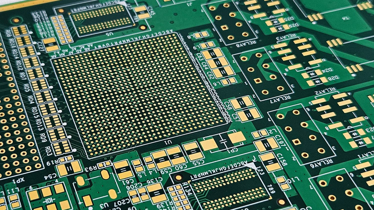
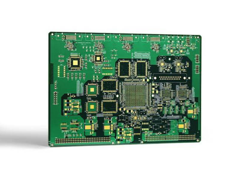
The clearest case is high-density interconnect. HDI builds depend on fine traces to fan out fine-pitch BGAs, and the routing density that makes HDI worthwhile is only achievable with tight line-and-space rules. Any-layer HDI pushes this further, since every layer carries fine routing rather than just the outer two. On an HDI PCB design, the foil specification is usually settled alongside the microvia and line-width rules, not separately.
The second case is mSAP. Semi-additive processing starts with a very thin electroless or laminated copper layer — often in the 2–5 µm range — images the trace pattern, plates the traces up to final thickness, then flash-etches the thin seed layer away. Because the final etch step only has to remove a few microns, there is essentially no undercut, and traces come out with near-vertical walls at widths that subtractive etching cannot hold. This is the process that makes 25 µm and finer line-and-space production viable.
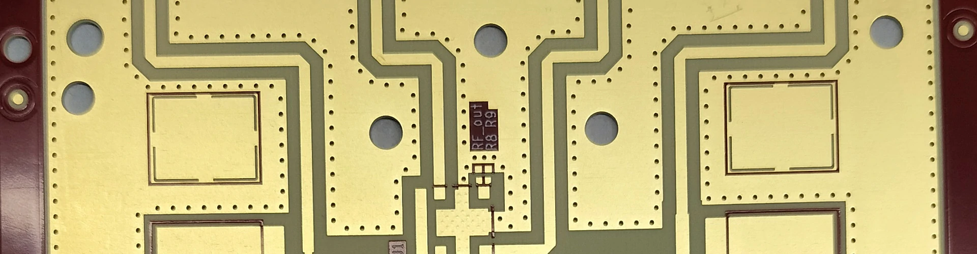
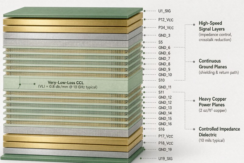
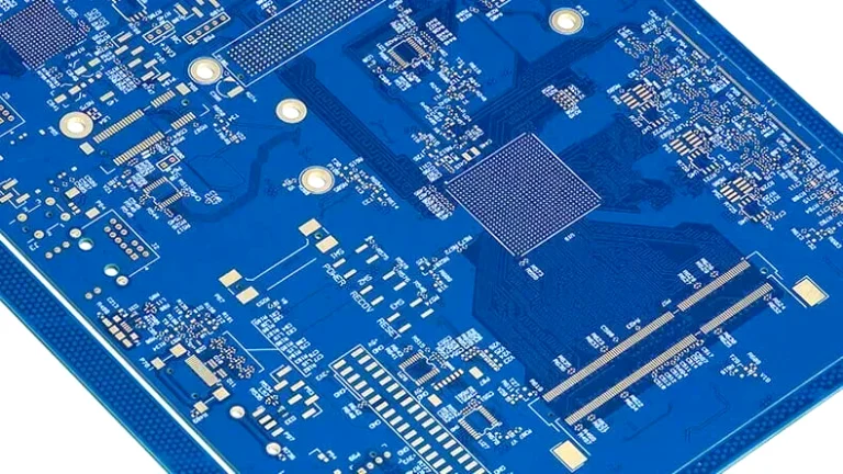
The third is high-speed design, though for a subtler reason. At high frequency, current flows in a thin layer at the conductor surface, and the roughness of the copper-to-dielectric interface contributes directly to conductor loss. Thinner foils used with appropriate surface treatment can reduce that contribution, which is one reason ultra-thin foil appears alongside low-loss laminates in high-speed PCB stackups.
A multilayer PCB that mixes requirements — fine-line signal layers plus power planes carrying real current — often ends up with different copper weights on different layers. That is normal, but it has to be specified clearly, because the fabrication flow has to accommodate both.
The Trade-offs: Handling, Current and Cost
Ultra-thin foil is not a free improvement, and in some designs it is the wrong choice.
Handling and yield. Thin foil wrinkles and tears far more easily than standard foil. Lamination, automated handling and even manual inspection all need adjusted procedures, and yield loss from foil damage is a real cost driver. Not every fabricator is equipped for it.
Current capacity. A trace on 12 µm copper carries less current than the same trace on 35 µm copper, and its DC resistance is higher. For power distribution or any net carrying meaningful current, thin foil is the wrong direction — this is where heavy copper belongs. The design rule is straightforward: thin foil on signal layers where geometry matters, thicker copper on power layers where ampacity matters.
Cost and availability. Ultra-thin and carrier-backed foils cost more than standard foil, are available from fewer suppliers, and typically carry longer lead times. On a cost-sensitive design with relaxed design rules, the premium buys nothing.
Process compatibility. Thin foil interacts with the rest of the process: oxide treatment, brown oxide, plasma desmear and plating all have to be tuned for it. A fabricator experienced with the specific construction is worth more than the material choice itself.
What to Specify When Ordering
A few items are worth settling explicitly, because ambiguity here tends to surface as a capability disagreement after the design is released:
- Foil thickness per layer, including whether power and signal layers use different weights.
- Whether the foil is carrier-backed, and at what stage the carrier is removed.
- Surface treatment or roughness profile, particularly if conductor loss matters for the design.
- Target finished line width and the tolerance the fabricator will hold at that foil thickness.
- Whether the process is subtractive or semi-additive, since that determines what is achievable.
- Confirmation that the specific laminate-and-foil combination is stocked — availability for PCB Raw Materials Library constructions in thin foil is narrower than for standard materials.
Raising these during DFM review is the cheapest way to resolve them. A design that specifies 12 µm foil and 25 µm lines needs a fabricator who can hold both together, and confirming that before tooling costs far less than discovering it on the first article.
Conclusion
Ultra-thin copper foil earns its place because it changes etch geometry rather than electrical properties. Less copper to remove means shorter etch time, less undercut and near-vertical trace walls, and that is what makes 25 µm and finer line-and-space reproducible. Where routing density or fine-pitch fan-out is the constraint, thin foil is effectively mandatory; where it is not, the premium buys nothing.
The trade-offs are equally specific: harder handling and lower yield, reduced current capacity, higher material cost and longer lead time, and a process that has to be tuned for it. The practical pattern is mixed copper weights — thin foil on the fine-line signal layers, thicker copper on the layers that carry current.
If you are evaluating whether a design needs ultra-thin foil, send the target line-and-space, layer count and current requirements, and we can advise on which foil and process combination actually supports it.
FAQ
What thickness counts as ultra-thin copper foil?
Generally 12 µm and below, corresponding to 1/3 oz or thinner. Below about 5 µm the foil is normally supplied on a carrier that is peeled away after lamination, because free-standing copper that thin cannot be handled without damage.
Does thinner copper foil reduce signal loss?
Indirectly. The main benefit is geometric — finer traces with vertical walls, which improves impedance accuracy. There is also a loss benefit when foil roughness is reduced, since conductor loss at high frequency is strongly influenced by the copper surface profile.
Can ultra-thin foil be used on power layers?
It is usually the wrong choice. Thinner copper means higher DC resistance and lower current capacity, so power and ground layers generally use thicker copper. Mixed copper weights across a stackup are common and normal.
Is ultra-thin foil required for mSAP?
Yes, in practice. Semi-additive processing depends on starting from a very thin copper layer, plating the traces up, and then flash-etching only a few microns. The minimal final etch is what produces the vertical trace walls that subtractive etching cannot achieve.