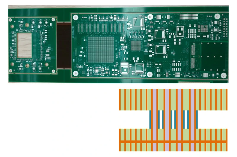
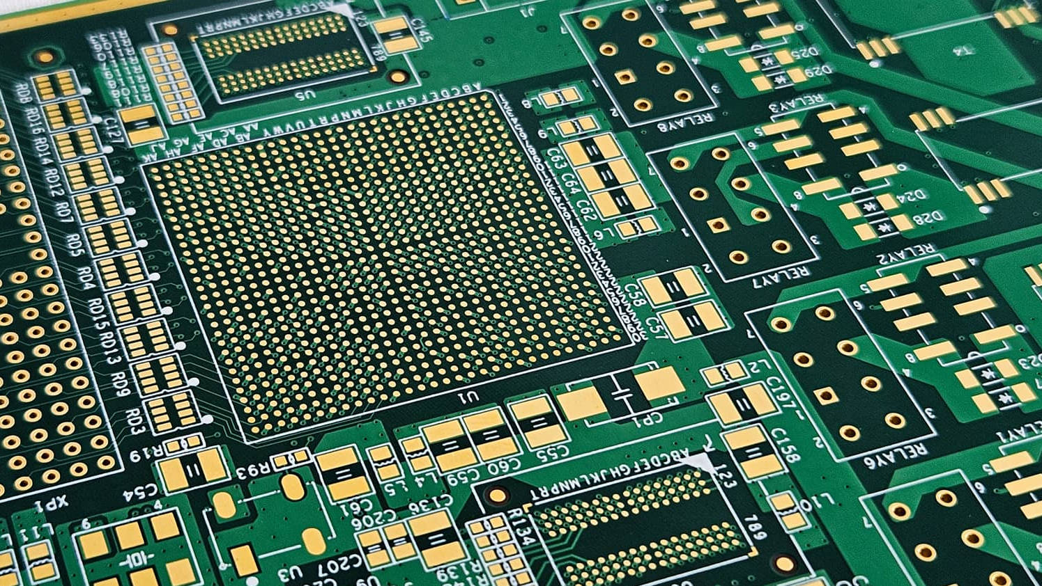
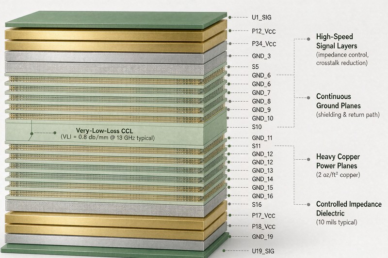
Via design in high-frequency PCBs affects impedance continuity, return path quality, signal loss, reflection, crosstalk, and EMI performance. In RF and high-speed layouts, vias should not be treated as simple vertical connections. Every signal via, ground via, via stub, pad, antipad, and reference-plane transition can influence signal integrity.
In low-speed circuits, a via may only need to provide electrical connection between layers. In high-frequency PCB layout, the same via can behave like a small transmission-line discontinuity. If the via stub is too long, the return path is poorly controlled, or ground vias are missing near RF transitions, the board may suffer from insertion loss, return loss, resonance, impedance mismatch, or unstable test results.
For engineering teams, the practical question is not “Can we use vias in high-frequency PCB design?” The better question is: where are vias necessary, how should they be structured, and which via-related risks should be reviewed with the PCB manufacturer before fabrication?
Mars-PCB supports high-frequency PCB DFM review for RF and high-speed circuit boards where via structures, stackup, controlled impedance, and fabrication capability must be checked before production.

Why Vias Become a Problem at High Frequency
A PCB via is a plated vertical interconnect. It connects one copper layer to another through a drilled hole. At lower frequencies, the via is often modeled simply as a connection. At higher frequencies, that simplified view becomes risky.
A high-frequency via can introduce:
| Via-Related Effect | What It Can Cause |
| Parasitic inductance | Impedance discontinuity and slower transition |
| Parasitic capacitance | Reflection and impedance mismatch |
| Via stub resonance | Return loss and signal attenuation |
| Return path disruption | EMI, radiation, and crosstalk |
| Pad and antipad discontinuity | Local impedance shift |
| Layer transition mismatch | Insertion loss and signal distortion |
| Poor ground via placement | Weak field control and higher noise coupling |
In high-frequency PCB design, a via is part of the signal path, not just a hole in the board.
This matters in RF PCBs, microwave PCBs, radar boards, antenna modules, high-speed backplanes, PCIe-related boards, telecom equipment, and other circuits where signal edges or operating frequencies make the layout electrically sensitive.
The Via Stub Problem: Small Structure, Large RF Effect
A via stub is the unused portion of a plated through-hole via that extends beyond the layer where the signal exits. For example, if a signal travels from the top layer to an internal layer, the remaining plated barrel below that internal layer becomes a stub.
This stub can behave like an unterminated transmission-line branch. At high frequency, it may reflect signal energy back into the main path and create resonance. Samtec notes that the via stub can start degrading a via transition before the most prominent resonant frequency because it adds capacitance to the launch.(The Samtec Blog)
What Via Stubs Can Do
| Problem | Practical Result |
| Reflection | Return loss increases |
| Resonance | Certain frequencies show strong degradation |
| Added capacitance | Launch impedance changes |
| Insertion loss | Signal energy is reduced |
| Eye diagram degradation | High-speed digital margin drops |
| Phase disturbance | RF matching and timing may shift |
A via stub becomes more critical as frequency rises, signal edge rate increases, or the unused via length becomes longer.
This is why via stub review is often necessary in high-frequency PCB DFM, especially for thick multilayer boards, high-speed interfaces, RF transitions, and microwave circuits.
Back Drilling: When and Why It Is Used
Back drilling, also called controlled depth drilling, is a fabrication process used to remove most of the unused conductive plating in a via stub. TI describes back-drilling as a PCB manufacturing process that removes undesired conductive plating in the stub section of a via.(Texas Instruments)
Back drilling is commonly considered when:
- A high-speed signal passes through only part of a thick board
- A via stub is long enough to affect signal integrity
- Return loss or insertion loss must be improved
- The design uses high-speed connectors or backplanes
- RF or microwave layer transitions need cleaner behavior
- Simulation or SI review identifies via stub resonance risk
However, back drilling is not a magic correction for all via problems. It adds manufacturing cost, requires accurate drilling registration, and usually leaves a residual stub. Samtec also notes that back drilling removes most of the stub, but a residual stub remains.(The Samtec Blog)
Back Drilling Decision Table
| Situation | Back Drilling May Help? | Engineering Note |
| Long unused through-hole stub | Yes | Common use case |
| Thick multilayer high-speed board | Often yes | Depends on data rate and via transition |
| Short via stub at moderate frequency | Maybe not necessary | Simulation or SI review helps |
| RF launch with strict return loss | Often worth reviewing | Connector and launch structure matter |
| Low-speed control signal | Usually unnecessary | Cost may not be justified |
| Blind/buried via already avoids stub | May not be needed | Depends on stackup |
Back drilling should be specified only after checking layer transition, residual stub, drill tolerance, pad size, and manufacturer capability.
For this reason, high-frequency PCB projects should include via transition details in the DFM review stage rather than waiting until fabrication starts.
Ground Vias: The Return Path Is as Important as the Signal Path
In high-frequency PCB layout, current does not simply travel along the signal trace. The return current follows the nearby reference plane. When a signal changes layers through a via, the return path may also need a controlled transition.
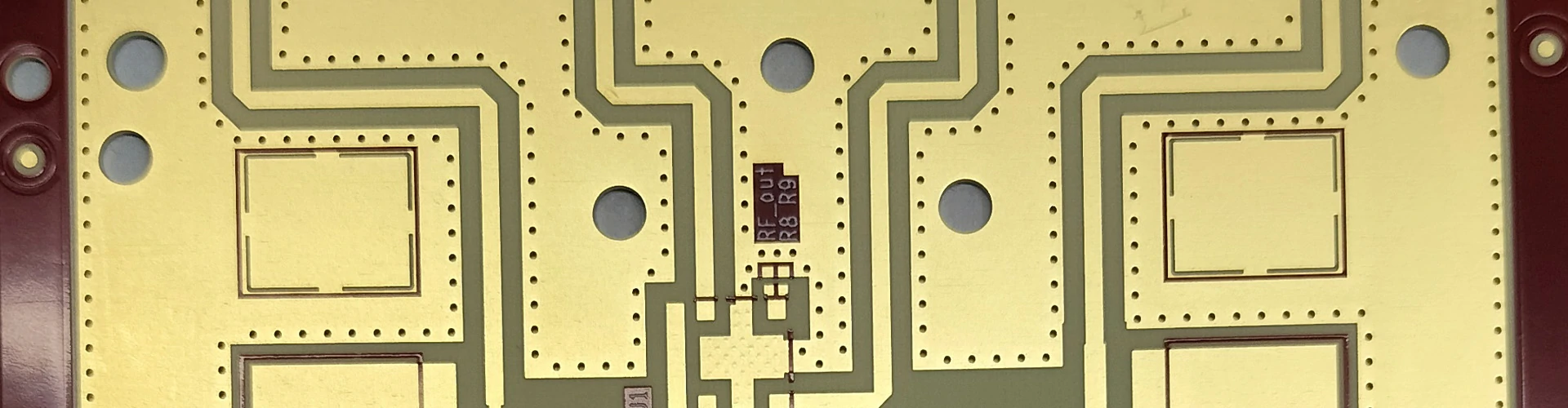
Ground vias are used to provide a nearby return path and help control electromagnetic fields around the signal via. In RF via design, ground vias are often placed near signal vias, connector launches, coplanar waveguide structures, and shielded RF regions.
Ground vias can help with:
- Return path continuity
- EMI reduction
- Crosstalk control
- Field containment
- Ground stitching
- Coplanar waveguide performance
- Connector launch stability
- Shielding between RF and digital regions
A common mistake is focusing only on the signal via while ignoring the return path. If the return current must detour around a plane split, slot, or missing ground connection, the via transition may radiate or create impedance discontinuity.
A high-frequency via transition should include both the signal path and the return path.
Signal Via, Ground Via and Antipad: What Should Be Reviewed
A via transition is not only the plated hole. It includes the pad, antipad, barrel, reference planes, and surrounding ground vias.
| Via Element | Why It Matters |
| Drill diameter | Affects barrel geometry and manufacturability |
| Finished hole size | Affects plating and via impedance |
| Pad diameter | Affects capacitance and annular ring |
| Antipad size | Controls clearance to reference planes |
| Barrel length | Affects inductance and possible stub length |
| Ground via distance | Controls return path and field coupling |
| Via-to-trace transition | Affects impedance continuity |
| Layer pair | Determines whether the stub is short or long |
| Plating thickness | Affects reliability and final geometry |
If the antipad is too small, capacitance to reference planes may increase. If the antipad is too large, return path continuity may weaken. If ground vias are too far away, the RF transition may become less controlled.
This is why high-frequency via design should be reviewed as a 3D structure, not just a 2D hole pattern.
Through-Hole, Blind, Buried and Microvias in High-Frequency PCB Layout
Different via types create different high-frequency behavior and manufacturing tradeoffs.
| Via Type | Description | High-Frequency Advantage | Key Concern |
| Through-hole via | Passes through entire board | Simple and widely manufacturable | May create long unused stub |
| Blind via | Connects outer layer to inner layer | Can reduce stub length | Higher process complexity |
| Buried via | Connects internal layers only | Saves surface routing and may reduce transitions | More complex lamination |
| Microvia | Small laser-drilled via, often for HDI | Short transition and compact layout | Reliability and stackup rules must be checked |
| Back-drilled via | Through-hole via with stub mostly removed | Reduces stub-related SI problems | Adds process step and residual stub remains |
For many high-frequency designs, the most suitable via type depends on the stackup. A through-hole via may be acceptable if the signal uses most of the barrel length. It becomes more problematic when the signal only travels a short distance and leaves a long unused stub.
Blind or buried vias can reduce stubs, but they may increase fabrication cost and complexity. Microvias can be useful in dense RF or high-speed designs, but they must be aligned with manufacturer capability and reliability requirements.
RF Via Design vs High-Speed Digital Via Design
RF via design and high-speed digital via design overlap, but they are not identical.
| Design Aspect | RF Via Design | High-Speed Digital Via Design |
| Main concern | Impedance, return loss, phase, RF transition | Eye margin, insertion loss, reflection, crosstalk |
| Common structure | Coaxial-like via, GCPW transition, via fence | Differential via pair, back-drilled connector launch |
| Return path | Ground vias close to signal transition | Reference continuity and stitching vias |
| Test metric | S-parameters, return loss, insertion loss | Eye diagram, jitter, S-parameters |
| Layout sensitivity | Very sensitive to field geometry | Sensitive to discontinuity and skew |
| Fabrication review | RF launch, antenna feed, shield via, stub | Back drilling, differential pair symmetry, via stub |
In both cases, vias should be included in simulation or at least reviewed for stackup compatibility. For RF and microwave layouts, via geometry may affect matching networks, antennas, and filter response. For high-speed digital layouts, via geometry may affect channel loss and reflection.
Where Via Problems Usually Appear on High-Frequency Boards
Via issues are most likely to occur in specific layout areas. These areas should be highlighted during DFM review.
| Layout Area | Common Via Risk |
| Connector launches | Stub, antipad, return path, ground via placement |
| BGA breakout | Dense vias, reference changes, impedance disruption |
| RF layer transitions | Signal discontinuity and poor grounding |
| Antenna feed networks | Phase mismatch and impedance shift |
| Grounded coplanar waveguide | Via fence spacing and ground stitching |
| High-speed differential pairs | Skew, asymmetry, and via stub |
| Mixed RF/digital regions | Noise coupling and poor return path |
| Power amplifier areas | Thermal vias interfering with RF fields |
A good high-frequency PCB layout review should not only ask whether the board can be fabricated. It should ask whether the fabricated via structure will preserve the intended signal behavior.
High-Frequency PCB DFM Review Checklist for Via Design
Before fabrication, engineers should prepare via-related information for the PCB manufacturer.
| DFM Review Item | What to Check |
| Stackup | Which layers do critical signals transition between? |
| Signal via type | Through-hole, blind, buried, microvia, or back-drilled |
| Stub length | Is the unused barrel length acceptable? |
| Back drilling | Is controlled depth drilling required? |
| Residual stub | What residual length is expected after back drilling? |
| Drill size | Is the via manufacturable with required tolerance? |
| Pad and antipad | Are capacitance and clearance balanced? |
| Ground vias | Are return vias close enough to the signal via? |
| Plane continuity | Is there a continuous reference path? |
| Impedance target | Is the via transition included in impedance/SI review? |
| Differential symmetry | Are paired vias balanced and length-matched? |
| Test requirement | Are impedance coupons or SI checks needed? |
For high-frequency PCB projects, Mars-PCB can provide high-frequency PCB DFM review to help check via structures, controlled impedance, material stackup, and fabrication feasibility before production.
Practical Layout Guidelines for High-Frequency Via Design
The following guidelines are not universal rules, but they are useful starting points for design review.
Keep Critical Signals on Fewer Layers When Possible
Every layer transition creates a via transition. If a critical RF or high-speed signal can stay on one layer without compromising routing or EMI, the design may avoid unnecessary via discontinuities.
Minimize Long Via Stubs
If a through-hole via creates a long unused barrel section, review whether back drilling, blind vias, buried vias, or stackup changes are appropriate.
Place Ground Vias Near Signal Vias
Ground vias can support return current transition and help control fields around signal vias. This is especially important for RF launches, coplanar waveguide structures, and shielded high-frequency regions.
Avoid Plane Splits Under Via Transitions
A signal via that crosses reference layers needs a controlled return path. Plane splits, slots, and large voids near the transition can create discontinuities and EMI risk.
Keep Differential Via Pairs Symmetrical
For high-speed differential pairs, the two signal vias should be as symmetrical as possible. Differences in geometry, spacing, or return path can create skew and mode conversion.
Mark RF-Critical Via Areas in Fabrication Notes
Connector launches, antenna feeds, RF transitions, and phase-sensitive paths should be identified clearly. This helps the manufacturer understand which via structures require closer review.
Common Mistakes in High-Frequency Via Design
Mistake 1: Using Through-Hole Vias Everywhere
Through-hole vias are simple and cost-effective, but they can create long stubs in multilayer boards. Critical high-frequency nets should be reviewed before through-hole vias are accepted by default.
Mistake 2: Adding Back Drilling Too Late
Back drilling affects pad design, drill planning, fabrication notes, and cost. It should be considered during stackup and layout planning, not added casually after files are finished.
Mistake 3: Ignoring Return Vias
A signal via without a nearby return via may create a return path discontinuity. This is a common cause of radiation and impedance disruption.
Mistake 4: Treating RF Via Fences as Decorative Grounding
Via fences need proper spacing, connection, and relationship to the RF structure. Random ground vias may not provide the intended field control.
Mistake 5: Not Asking the Manufacturer About Residual Stub
Even with back drilling, some residual stub remains. The expected residual stub should be confirmed with the PCB manufacturer and considered in SI review.
What to Send Your PCB Manufacturer for Via Review
A simple Gerber package may not fully explain via design intent. For high-frequency PCB fabrication, provide additional notes.
| Information to Provide | Why It Helps |
| Stackup drawing | Shows layer transitions and stub risk |
| Critical net list | Identifies RF or high-speed signals |
| Via type requirement | Defines through-hole, blind, buried, or back-drilled vias |
| Back drilling notes | Specifies controlled depth requirements |
| Impedance table | Helps review via transition impact |
| Ground via strategy | Clarifies return path and shielding intent |
| Connector launch details | Important for high-frequency interface transitions |
| Material and thickness | Affects via geometry and signal behavior |
| Test requirements | Defines impedance or signal integrity checks |
A qualified PCB manufacturer should be able to review whether the via structures match fabrication capability and whether any DFM risks may affect signal integrity.
For broader PCB production support, engineers can also review Mars-PCB custom PCB manufacturing when planning prototype, pilot run, or production requirements.
FAQ
What is via design in high-frequency PCB layout?
Via design in high-frequency PCB layout refers to planning signal vias, ground vias, via stubs, pads, antipads, and layer transitions so that impedance, return path, signal loss, and EMI behavior remain controlled.
Why are via stubs bad for high-frequency PCBs?
Via stubs can act like unterminated transmission-line sections. At high frequencies, they may cause reflection, resonance, return loss, insertion loss, and signal distortion.
What is back drilling in PCB manufacturing?
Back drilling is a controlled-depth drilling process used to remove most of the unused conductive plating in a via stub. It is commonly used in high-speed and high-frequency PCBs to reduce stub-related signal integrity problems.
When should back drilling be used for high-frequency PCBs?
Back drilling should be considered when a through-hole via creates a long unused stub on a critical RF or high-speed signal. The decision should depend on frequency, board thickness, layer transition, stub length, and signal integrity requirement.
Why are ground vias important in RF via design?
Ground vias provide a nearby return path and help control electromagnetic fields around signal vias. They can reduce radiation, improve shielding, support coplanar waveguide structures, and reduce impedance discontinuity.
Are blind vias better than through-hole vias for high-frequency PCB design?
Blind vias can reduce via stub length and improve routing density, but they increase fabrication complexity and cost. They are not always better; the best via type depends on stackup, frequency, reliability, and manufacturing capability.
What should be checked in high-frequency PCB DFM review?
A high-frequency PCB DFM review should check stackup, critical signal transitions, via stub length, back drilling needs, drill size, pad and antipad geometry, ground via placement, reference plane continuity, impedance targets, and test requirements.
Conclusion
Via design is one of the most overlooked but important parts of high-frequency PCB layout. Signal vias, via stubs, ground vias, back drilling, pad geometry, antipads, and return paths all influence impedance continuity, signal loss, reflection, crosstalk, and EMI behavior.
For engineering teams, the safest workflow is to review via design together with stackup, controlled impedance, material selection, and fabrication capability before sending files to production. This is especially important for RF PCBs, microwave boards, radar modules, high-speed interfaces, and dense multilayer designs.
Mars-PCB supports high-frequency PCB DFM review for projects that require via structure review, controlled impedance support, RF material selection, and high-frequency PCB manufacturing feedback.