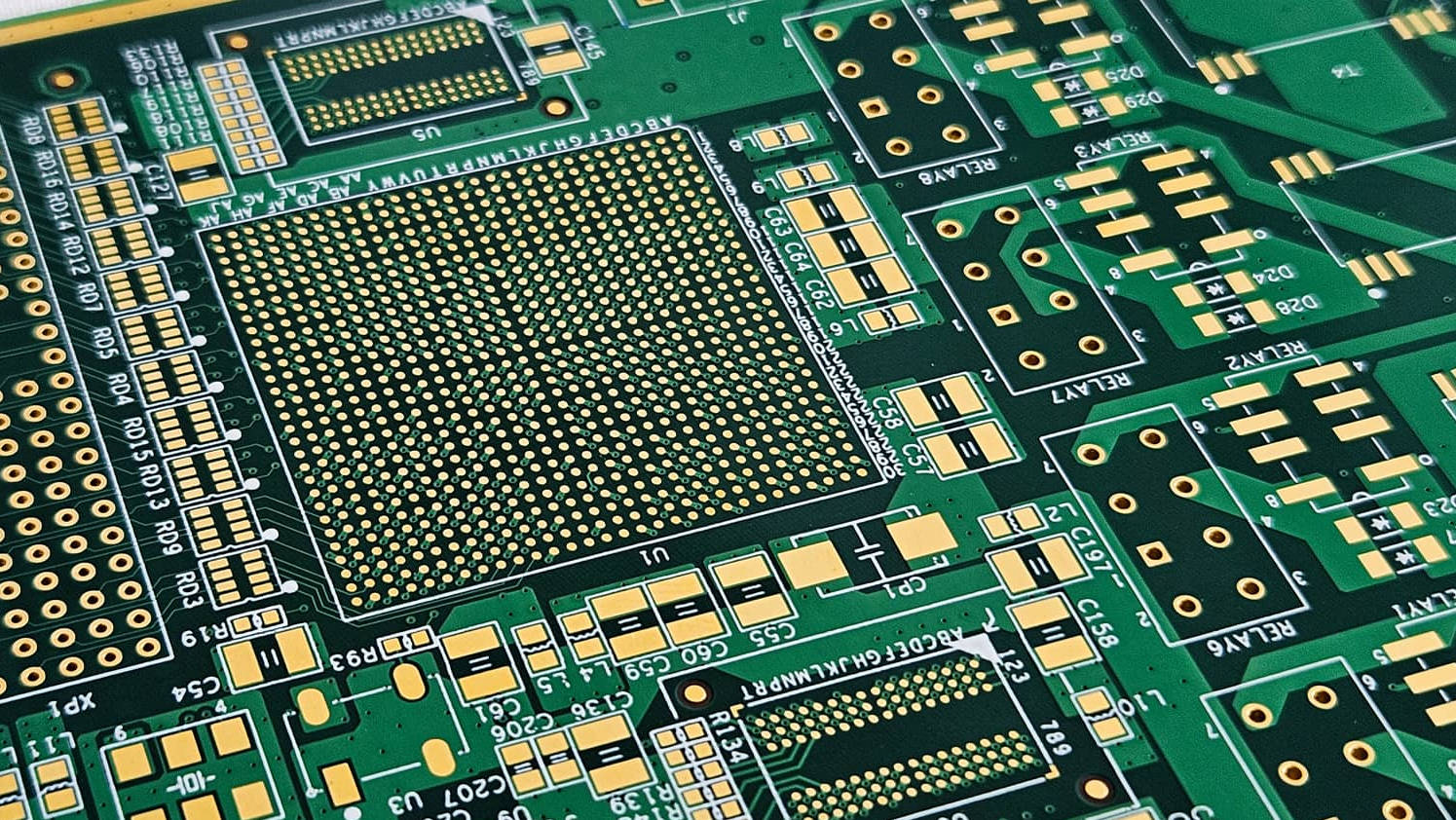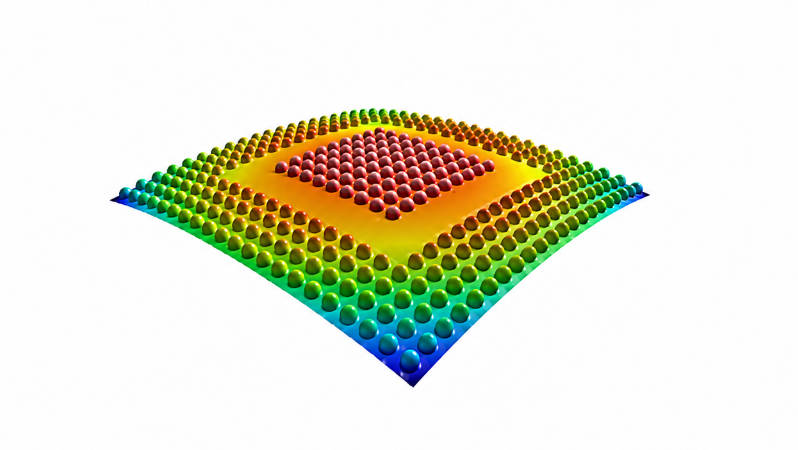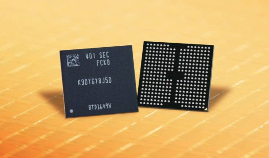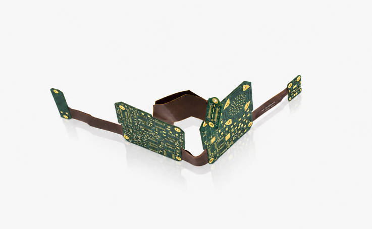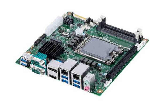
If you are designing or sourcing a PCB for an AI server, three decisions usually settle whether the board will hold up at 100 Gbps-class signaling and several hundred watts of socket power: layer count, base material, and impedance control. Get any of the three wrong and you either lose signal integrity on the high-speed serial links or you cannot deliver current to the accelerator die. This guide explains how each decision is typically made for AI server boards, the trade-offs to expect between them, and the specifications worth pinning down before you issue an RFQ.
Why Layer Count Matters in AI Server PCBs
AI servers concentrate two requirements that rarely appear together in conventional designs: very high signaling rates on the longest nets, and high DC current drawn by GPUs, NPUs, or switch ASICs. A typical AI server motherboard or accelerator card routes PCIe Gen5 or Gen6 between the host CPU and the accelerator, multiple 100 GbE, 400 GbE, or 800 GbE ports to the fabric, DDR5 channels that require strict length matching, and high-current power planes feeding sockets that draw several hundred watts each. Each of those needs wants a different layer in the stack. PCIe Gen5 routing wants short signal layers that reference a solid ground. DDR5 wants tightly length-matched stripline layers with controlled skew. Power delivery wants thick copper planes close to the component side. Once all of those needs are accounted for, the stackup stops being a four- or six-layer exercise and starts resembling 16, 20, or more layers in a typical multilayer PCB build.
Common Layer Count Ranges and Where They Fit
The exact layer count depends on the AI server SKU, the channel count per ASIC, and whether the board is a host board, an accelerator module, or a switch fabric board. The table below summarizes the ranges that are typically considered for each class of board. A specific design may need more or fewer layers depending on its architecture.
| Board Class | Typical Layer Count Range | Main Drivers |
|---|---|---|
| AI accelerator card (PCIe form factor) | 12 to 18 layers | High-speed serial lanes to host, dense power delivery to GPU or NPU |
| AI server host board (single or dual socket) | 16 to 24 layers | Multiple PCIe lanes, DDR5 channels, high-current VRM planes |
| AI training cluster switch board | 20 to 30+ layers | Very high SerDes density, longest matched pairs, many power domains |
| AI inference appliance motherboard | 14 to 20 layers | Balance of cost and channel count, often lower signaling rate than training |
These ranges are general rather than fixed. A design may need additional layers for back-drilling stub control, for separate high-speed and low-speed reference planes, or for embedded capacitance layers. Where the layer count is not yet settled, it helps to prototype the stackup with the fabricator’s field solver before committing to a bill of materials.
Stackup Design Principles That Apply Across AI Server Boards
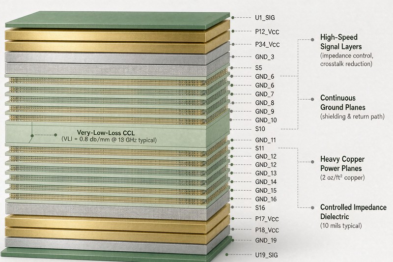
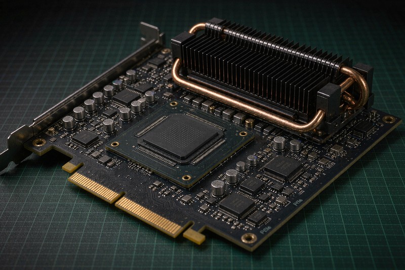
A few stackup principles tend to apply regardless of the exact layer count. The stack should be symmetric around its center to limit warpage during lamination and reflow; asymmetric builds look easier on paper and usually cause problems at reflow. Each high-speed signal layer should reference a solid ground plane rather than a power plane, which reduces return-path discontinuities. Tighter dielectric spacing between signal layers improves high-frequency loss and allows tighter via-to-via pitch, but it raises lamination complexity and cost. It is common to plan at least two heavy copper planes, typically 2 oz or 3 oz, close to the top side where the ASIC sits, because AI accelerator sockets draw high current at low voltage. Where the longest nets exceed roughly 5 Gbps, leave room in the stack for back-drilled vias to remove stubs that would otherwise resonate in the Nyquist band.
Material Selection for the High-Speed Layers
The base material chosen for the high-speed signal layers affects signal integrity more than the layer count itself. The loss tangent and dielectric constant of the laminate determine how much the eye opening shrinks as the data rate rises.
In practice, AI server designs fall into a few material tiers. Standard and mid-loss FR-4 derivatives are generally adequate for PCIe Gen4 and lower, and are marginal for Gen5 at longer reaches. Low-loss FR-4 family materials are a common choice for AI server host boards running Gen5 or moderate-length Gen6. Very-low-loss CCL, often referred to by industry shorthand as M6, M7, or M8 grade material, is used on the longest channels, the SerDes layers, and anywhere the link budget is tight.
The grade that fits depends on the longest reach and the channel loss budget set by the SerDes IP vendor. Moving from a low-loss to a very-low-loss material can extend reach for a given signaling rate, and it also raises cost, so the usual approach is to use very-low-loss material only on the layers that carry the longest, fastest signals and a less expensive material on the remaining layers. Material availability is a real constraint in 2026; lead times on the highest-grade CCL have stretched, so specifying a material that is hard to source can disrupt a program schedule more than a tight impedance target. The exact loss and cost figures should be confirmed with the laminate supplier for the specific grade in question.
For a structured overview of currently stocked high-speed CCL grades, including M6, M7, and M8 families, the PCB raw materials library is a useful starting point. The exact loss, cost, and availability figures for any specific grade should still be confirmed with the laminate supplier.
Impedance Control and Signal Integrity
AI server boards are impedance-controlled boards. Every high-speed trace is designed to a target impedance, commonly 85 or 100 ohm differential for SerDes and PCIe, and 50 ohm single-ended for certain clock and single-ended interfaces. The fabricator is expected to hold that impedance within a stated tolerance, which on most layers is around plus or minus 10 percent and tighter, around 8 percent, on the critical SerDes layers.
Stackup affects impedance as much as trace geometry, so a fabricator cannot hit a 90 ohm differential target on a stack where the dielectric spacing between the signal layer and its reference plane is wrong. Surface copper profile also matters; reverse-treated foil and very-low-profile copper reduce conductor loss at high frequency, which becomes significant for 112 Gbps and 224 Gbps SerDes. Resin content and glass style shift the effective dielectric constant enough to push a target impedance out of spec, so it is worth asking the fabricator which glass style will be used on each layer. Coupon testing is standard practice on AI server builds, with impedance coupons on every panel and time-domain reflectometry verification at coupon test on the critical layers.
Thermal and Power Delivery Considerations
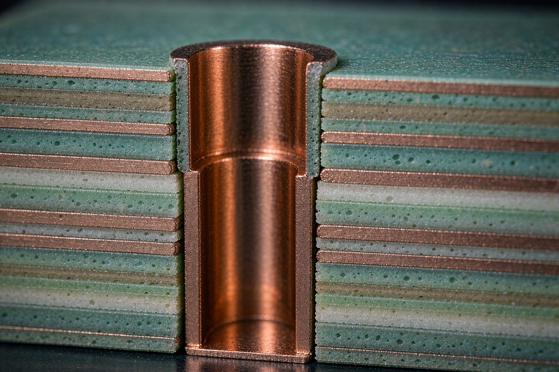
The high layer counts on AI server boards exist partly to deliver clean power and to spread heat. Two-ounce copper on each power plane is common, and three-ounce and above (typically classed as heavy copper) appear on the most demanding accelerator boards, though heavier copper raises fabrication cost and can reduce yield on fine-line layers. Arrays of filled and plated-over thermal vias under the BGA package of the accelerator pull heat into inner copper planes and toward the heatsink interface, so via diameter, fill material, and cap plating should be specified up front rather than left to default. Some AI server designs separate analog and digital ground planes and join them at a single point; where that is done, the stackup has to support the split.
Common Mistakes When Specifying AI Server PCBs
A number of mistakes show up when AI server designs return from prototyping with signal-integrity or power-integrity problems. Treating layer count as a cost variable to be minimized usually costs more in signal-integrity rework than it saves in laminate. Specifying an impedance target without specifying the stackup leaves the fabricator without a workable reference. Using the same material on every layer ignores that most AI server designs benefit from a hybrid stack. Forgetting back-drilling lets stubs resonate and close eye openings at high data rates. Underestimating via-to-via pitch on dense BGAs leads to capture-pad-to-drill ratios that many fabricators struggle to hold. Specifying finished copper without specifying the starting copper profile leaves the surface treatment to chance.
Most of these issues are caught earlier in the supplier’s DFM review, and requesting a written DFM report alongside the RFQ usually aligns the stackup, materials, and impedance expectations before tooling.
Specification Checklist Before You Send an RFQ
Before sending an RFQ for an AI server PCB, the following items are worth pinning down in the fabrication notes or in a separate stackup drawing:
- Total layer count with a stackup drawing
- Per-layer material grade and glass style
- Finished copper weight on every layer
- Target impedance and tolerance on each controlled layer
- Maximum via stub length or an explicit back-drilling depth
- Thermal via pattern under each high-power BGA
- Surface finish on the high-speed BGA pads
- Acceptable panel size and units per panel
- Required inspection coupons
- Acceptance standard, whether IPC Class 2 or IPC Class 3
If several of these are missing, a supplier will typically quote to defaults that are reasonable for ordinary designs but often wrong for AI server boards. Confirming them before the quote avoids a redesign cycle later.
Conclusion
For AI server PCBs, layer count, base material, and impedance control are not independent decisions. They have to be planned together against the signaling rate, the longest reach, the current drawn by the accelerator, and the channel loss budget set by the SerDes vendor. The layer count follows from the mix of high-speed, matched-length, and high-current requirements the board has to carry. The material split follows from how much loss the longest channels can tolerate. The impedance and back-drilling approach follows from the stackup and the glass style that the fabricator will actually use. A stackup that closes the signal-integrity eye, delivers current to the ASIC without excessive IR drop, and can be sourced within the program schedule is the practical target; optimizing any one of those three in isolation usually costs more than it saves.
If you have a target signaling rate, an expected layer count, and a power budget for your AI server board, share those requirements with the Mars PCB engineering team. We can review your stackup, recommend a material split across layers, and confirm the impedance and back-drilling approach that fits your channel loss budget and your program schedule.
FAQ
What is the typical layer count for an AI accelerator card?
Most PCIe-form-factor accelerator cards fall in the 12 to 18 layer range. The exact number depends on the channel count to the host, the power delivery needs of the ASIC, and whether back-drilling is required.
Do all layers in an AI server PCB need the highest-grade material?
No. Most AI server designs use a hybrid stack, with very-low-loss material on the longest and fastest signal layers and a less expensive material on the slower layers and on the power and ground planes.
Is back-drilling always required on AI server boards?
It is required on most boards running high-baud-rate signaling where via stubs would resonate in the band of interest. At lower rates, stubs are often short enough not to matter, but the decision should still be evaluated channel by channel.
Can standard FR-4 be used in an AI server PCB?
Standard FR-4 is generally not suitable for the high-speed signal layers on boards running PCIe Gen5 or faster signaling, because loss and dielectric constant stability are insufficient. It may still be acceptable on power layers and on layers that carry only low-speed signals.
What is the difference between M6, M7, and M8 grade CCL?
These are industry shorthand labels for very-low-loss CCL grades with progressively lower loss tangent and higher cost. The right grade depends on the longest reach in the design and the channel loss budget set by the SerDes IP vendor.
How is impedance tolerance usually specified on AI server PCBs?
Target impedance is typically specified per controlled layer, commonly 85 or 100 ohm differential for SerDes and PCIe and 50 ohm single-ended for certain interfaces. Tolerance is usually around plus or minus 10 percent on most layers and tighter, around 8 percent, on the critical SerDes layers, verified through coupon testing.