Designers who push trace and space below 50 micrometres run into a wall with conventional subtractive etching: the copper foil is already thicker than the trace you want to resolve, and the wet etch that forms the line starts to eat sideways faster than it goes down. Modified semi-additive processing (mSAP) sidesteps that problem by plating the trace upward from an ultra-thin copper base, which is why HDI PCB programs in AI server backplanes, high-speed network switches and substrate-like interposers now use mSAP as the default fine-line route. This article explains how the two processes work, where each one still makes sense, and how to decide between them before you commit the stack-up.
What Are Subtractive Etching and mSAP? Defining the Two Processes
Subtractive etching is the long-standing industry default. The fabricator starts with laminate already clad in copper — historically 1 oz (35 µm), then progressively thinner 1/2 oz (17 µm) and 1/3 oz (12 µm) foils to give finer resolution. Photoresist is laminated, exposed and developed to leave an etch mask, and the exposed copper is then dissolved in an etchant bath. The line geometry is defined entirely by how cleanly the etchant removes copper around the mask.
mSAP (modified semi-additive processing) takes a different starting point. The laminate is clad with an ultra-thin copper base — typically 5 µm to 9 µm, with 3 µm under active development. A thin plating resist is patterned, then copper is electroplated upward into the openings to the target trace thickness (often 15 µm to 25 µm). A short flash-etch step removes the thin sacrificial copper between the plated traces, the resist is stripped, and the result is a line whose profile is controlled by plating rather than by etch.
The practical difference is in who defines the line geometry. Subtractive etching is “what the etchant leaves behind”; mSAP is “what the plating builds up”. For trace widths at or below 50 µm (2 mil), that subtle distinction decides whether the line is rectangular and impedance-stable, or trapezoidal with undercut that hurts insertion loss and timing margin.
Process Flow Comparison: Steps and Equipment
On paper, both routes look similar — coat, expose, develop, shape copper, strip. In practice the equipment, inspection gates and yield-driving risks are quite different. The table below summarises the steps each fab actually runs through.
| Step | Subtractive Etching | mSAP |
|---|---|---|
| Starting copper foil | 12–35 µm clad CCL | 3–9 µm clad CCL or RCC |
| Imaging | Conventional UV exposure or LDI on dry film | LDI on thin plating resist (typical 10–25 µm) |
| Copper shaping | Wet alkaline or cupric chloride etch (chemical removal) | Electrochemical flash etch + copper electroplating |
| Etch depth sensitivity | Drives undercut, sensitive to etch factor | Flash etch is shallow and tightly controlled |
| Line profile | Trapezoidal, sidewall angle ~70–80° | Near-rectangular, sidewall angle ~85–90° |
| Typical minimum trace/space | 75 µm / 75 µm (3 mil / 3 mil) standard; 50 µm / 50 µm at the limit | 25 µm / 25 µm (1 mil / 1 mil) production, 20 µm / 20 µm advanced |
| Process inspection gates | AOI after develop + after etch | AOI after develop, plating-thickness metrology after plate, AOI after strip |
| Cycle-time adder vs conventional | Baseline | +1 plating step + resist strip; offset by parallel plating |
Two pieces of equipment tend to define whether a fab can run mSAP at all: a reliable LDI imager with sub-10 µm overlay accuracy, and a vertical or horizontal electrolytic plating line with tight current distribution control. Without both, 25 µm lines go from challenging to impossible — regardless of how thin the base foil is.
Why Fine-Line PCBs Are Moving to mSAP
The shift to mSAP is driven by four converging factors: line/space density, yield, signal integrity and stack-up headroom.
First, the density ceiling. At 17 µm starting copper, a 35 µm trace leaves roughly 30 µm of copper to remove on each side during etching. Even with optimised chemistry, the etchant removes sideways copper almost as fast as it removes top copper, producing a measurable undercut. By the time the line is fully isolated, the original photoresist opening has widened by 5–10 µm per side. Push the design to 25 µm trace on 12 µm copper, and the undercut alone consumes a third of the line. mSAP avoids this by plating the trace up from a 5 µm base — there is no deep etch, so the line profile stays close to rectangular.
Second, yield. Sub-50 µm subtractive etch panels routinely show footing, mouse-bite defects and differential etch bias across the panel. mSAP yields are dominated by plating-thickness uniformity and resist adhesion — both are easier to control in production than the chemistry of fine-line wet etch.
Third, signal integrity. Vertical sidewalls and rectangular cross-sections give a more predictable impedance profile along the line. For high-speed PCB channels at 28 Gbps, 56 Gbps or 112 Gbps PAM4, a 5% impedance tolerance is much easier to hit when the trace geometry is plating-defined than when it is etch-defined. This is one of the reasons mSAP is now standard in AI server backplanes and switch-fabric PCBs.
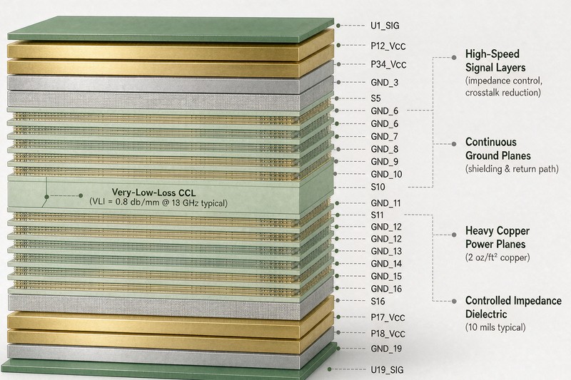
Fourth, material headroom. mSAP starts with thinner CCL, which means the fabricator can pack more signal layers into a fixed total board thickness — useful when the design calls for 4 mil line/space on a 0.8 mm stack. The right dielectric and copper-foil combination has to be selected from the start, which is where a project benefits from working against an established PCB raw materials library rather than reinventing the stack-up by trial and error.
When Subtractive Etching Still Wins
mSAP is not a universal upgrade. There are several situations where the conventional route remains the better choice.
Cost per panel. Sub-25 µm designs are not the norm in the B2B market, and for mainstream 4 mil / 4 mil HDI on 12 µm copper, the unit cost of subtractive etch is hard to beat. If your design is at 75 µm / 75 µm or above, asking for mSAP usually just adds plating cycles without giving you anything you actually need.
Heavy copper and power electronics. Designs that require 2 oz, 3 oz or thicker copper on inner or outer layers are still subtractive by necessity — there is no economical way to electroplate several ounces of copper onto a thin plating resist. If your design includes heavy copper PCB sections, expect the rest of the panel to follow conventional flow.
Total thickness and substrate. Very thick boards above 2.4 mm, ceramic PCBs and metal-core boards are not standard mSAP candidates. Process stability and the limited availability of ultra-thin-foil-clad cores for these constructions keep subtractive etching as the default.
Low-density legacy designs. Single-sided, double-sided and low-layer-count multilayers do not need mSAP. The extra capex burden only makes sense where the fine-line benefit actually shows up in the finished product.
Decision Framework: Choosing the Right Process
Use the matrix below as a starting point. Real-world designs always have at least one cell that disagrees with the table — that is normal, and the decision usually goes to whichever row drives the most cost or risk.
| Design Driver | Default Choice | Why |
|---|---|---|
| Trace/space ≥ 75 µm / 75 µm, low layer count | Subtractive | Lowest unit cost, broadest material availability |
| Trace/space 50 µm / 50 µm, ≤ 6 layers, low volume | Subtractive (close to the limit) | Avoids plating tooling setup for small batches |
| Trace/space 50 µm / 50 µm, 8+ layers, stacked microvias | mSAP | Stacked vias + fine lines together tip the balance |
| Trace/space ≤ 35 µm / 35 µm, any layer count | mSAP | Subtractive etching is no longer consistent at this resolution |
| Sub-1 oz copper + 5% impedance tolerance on long traces | mSAP | Plating-defined geometry gives better impedance control |
| ≥ 2 oz copper on any layer, including mixed builds | Subtractive | mSAP is uneconomical for thick copper |
| Ceramic, metal-core or aluminium-base construction | Subtractive | Limited ultra-thin-foil-clad options for these cores |
Once the matrix points to a process, run the choice past DFM review before locking the fab. The DFM team can confirm whether the proposed trace/space is actually inside the panel’s process capability window (often different from the headline data sheet), validate impedance margin against the stack-up dielectric constant, and flag whether via-in-pad copper fill, back-drilling or hybrid builds create hidden rework risk. For designs that touch controlled impedance budgets, this review should happen before artwork release — not after the first prototype comes back.
Conclusion
Subtractive etching remains the right process for designs that stay at 4 mil / 4 mil and above, for heavy-copper builds and for ceramic or metal-core substrates. mSAP becomes the better choice as soon as the trace/space pushes below 50 µm, the layer count exceeds six with stacked microvias, or the design needs a tight impedance window across long high-speed traces. For programmes that mix fine-line HDI areas with thicker-copper power or RF sections, the safest approach is to treat the two regions as separate sub-designs and route them through the appropriate process flow, accepting the extra panel-handling cost in exchange for a cleaner yield story on each side.
FAQ
Does mSAP fully replace subtractive etching?
No. mSAP replaces subtractive etching for fine-line and high-density regions of the PCB. Broader segments of the market — heavy copper, ceramic substrates, low-density multilayers — still run on conventional subtractive flow because mSAP adds plating and inspection steps that do not pay back in those constructions.
Can mSAP deliver 25 µm or 1 mil line/space in production today?
Yes, 25 µm / 25 µm is in production at fabs that combine LDI imaging with vertical continuous plating. Going below 20 µm / 20 µm is possible but requires tighter process control, sub-3 µm base foil and additional metrology — confirm this capability window with the fab before designing to it.
What does mSAP demand from the CCL (copper-clad laminate)?
The base foil has to be thin enough that the flash etch step fully removes the unwanted copper between plated traces without disturbing the rest of the stack. CCLs with 5–9 µm-treated or -untreated copper foils are the practical starting point. The exact dielectric and resin system should match the impedance profile and Tg requirements of the rest of the build.
When should we choose mSAP from day one?
Choose mSAP early when the stack-up, layer count or impedance budget leaves no margin for etch-driven line widening. This includes dense HDI designs with stacked microvias, AI server backplanes with sub-50 µm lines, and any board where controlled-impedance traces run more than a few centimetres. Waiting until the second prototype revision usually costs more than the early DFM conversation.