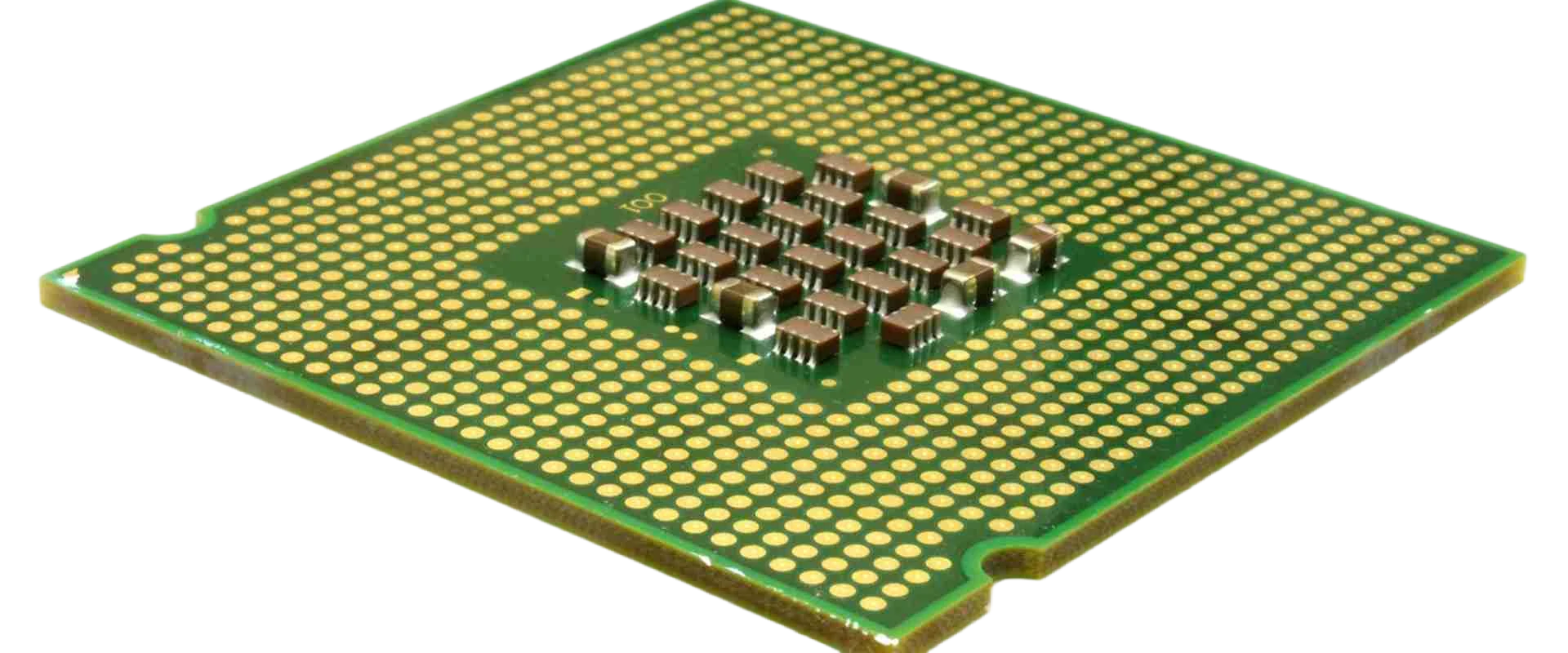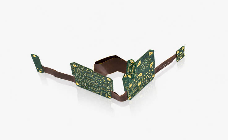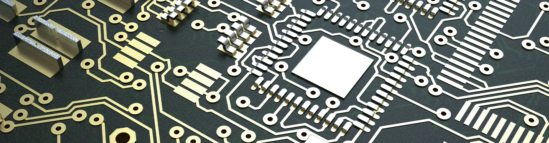
Chiplet architecture moves the hardest interconnect problems off the die and onto the package. Instead of one large monolithic processor, a design is split into several smaller dies that talk to each other through an interposer or a bridge. For board designers and PCB buyers that shift matters a great deal: the fine-pitch wiring that used to live inside a chip now lives on an interposer or an IC Substrate, and everything below it — the board, the power network, the thermal path — has to be re-thought around that.
The practical consequence is that the board is no longer designing to a single known component. It is designing to a stack: die, interposer, package substrate, solder balls, and then the PCB. Each layer in that stack has its own tolerance, its own expansion behaviour, and its own cost driver. This article walks through what changes at each level and what to confirm before you release a chiplet-based design to fabrication.
Why the Interconnect Moved Out of the Die
A monolithic SoC puts every function on one piece of silicon, and the traffic between those functions is carried by on-die metal layers — the finest and cheapest interconnect in the entire system. That is why large dies stayed attractive for so long despite poor yield: one die meant no off-chip penalty for internal bandwidth.
Chiplets invert the trade-off. Splitting a design into smaller dies improves yield, lets different functions sit on different process nodes, and makes it possible to reuse a proven die across several products. But the traffic between those dies now has to cross a physical boundary. In a 2.5D design that boundary is bridged by an interposer — usually silicon, sometimes organic — that sits between the dies and the package substrate. In a 3D design the dies stack vertically and the connection is a through-silicon via or a direct copper-to-copper bond.
Either way the interconnect burden moves down the stack. It lands on the package first, and whatever the package cannot absorb lands on the board.
The Interposer Is the New Critical Layer
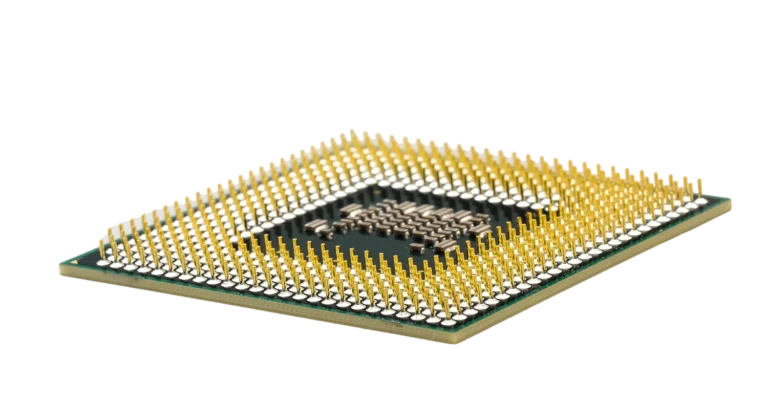
In a 2.5D assembly the interposer is doing work that used to be done on silicon. It has to route a very large number of die-to-die connections at a pitch far below anything a conventional board can produce. That is a fabrication capability question before it is a layout question: the process window of the interposer and of the substrate beneath it sets the limit before your layout team opens the tool.
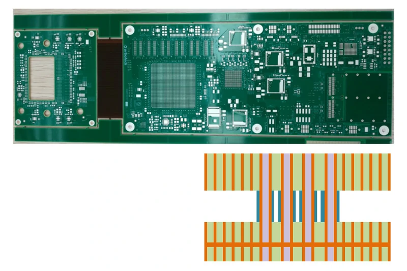
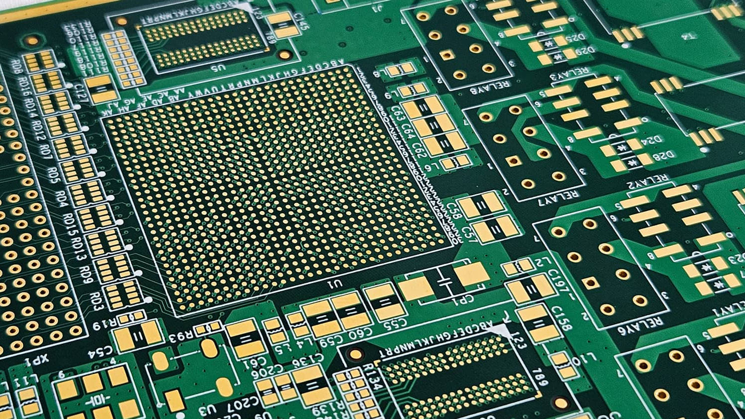
This is the same reason HDI PCB technology exists. When escape routing gets finer than through-hole or standard microvia processes allow, the manufacturing method has to change, not just the design rules. Chiplet packaging pushes that boundary several steps further down, and the board underneath has to absorb the result — more pins in the same footprint, tighter ball pitch, and less room for escape routing than a comparable monolithic part needed.
For the PCB buyer, the immediate effect is that the board’s own capability window becomes a gating item much earlier in the project. Routing density, microvia type, and layer count are no longer decisions that can wait until the schematic is frozen.
Bump Pitch Sets the Real Floor
Every level of the stack has its own feature scale, and confusion between them is one of the most common sources of late design changes. The table below is a qualitative map, not a specification — actual numbers vary by supplier, generation and package type, and must be confirmed against your vendor’s current capability.
| Level | What it carries | What constrains it |
|---|---|---|
| Die-to-die (interposer or bridge) | Parallel die-to-die links | Interposer process capability |
| Die-to-package (bump / pillar) | Power and signal into the substrate | Bump pitch and substrate line/space |
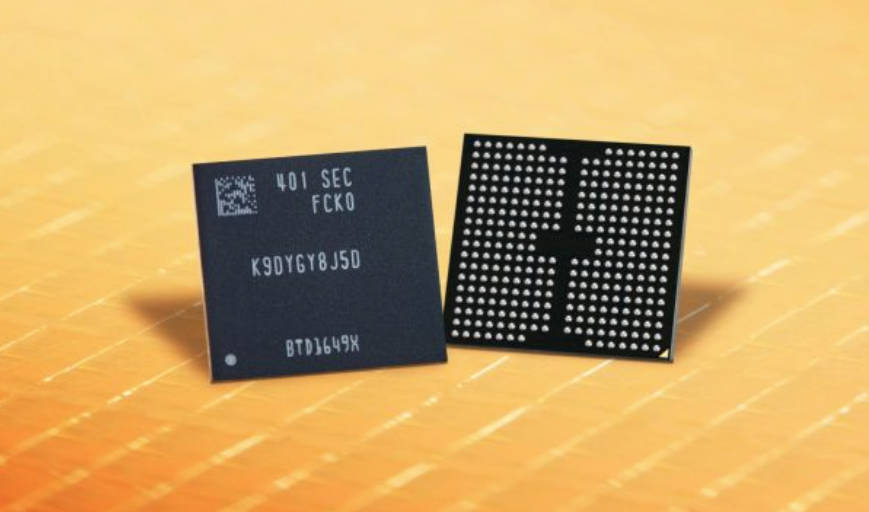
| Package-to-board (ball) | Everything the board sees | Ball pitch, board escape routing |
| Board-level routing | Distribution across the PCB | Fabrication capability of the PCB |
The important point for board designers is that the coarsest level sets the pin count they have to deal with, while the finest levels set the cost and the yield risk they inherit. A chiplet package may present a ball pitch that looks manageable, but the escape routing underneath it can still be severe, because the balls are dense and the signals leaving them are not evenly distributed.
Signal Integrity at the Package-to-Board Boundary
Die-to-die links on an interposer are short and controlled. The moment a signal leaves the package and enters the board, it enters a much less forgiving environment: longer traces, vias with stubs, connectors, and in many cases a connector-to-connector path across a backplane or a cable.
Chiplet-based accelerators are usually deployed in exactly the environments where High Speed PCB discipline already applies. That means the board design has to account for loss budget, reference-plane continuity, and via transitions with the same rigour as any high-speed design, and it has to do so with less routing space than before. Where a previous generation spread high-speed pairs across many layers, a dense chiplet package may force them into fewer layers with tighter spacing, which raises crosstalk risk.
Back-drilling, via-in-pad, and careful antipad design stop being optional refinements and become baseline requirements. The earlier those constraints are written into the stack-up, the fewer respins the project needs.
Power Delivery From the Board to the Bump
High compute density in a small footprint produces a power delivery problem that is harder than the signal problem. Current has to travel from the voltage regulator, through the board, through the package balls, through the substrate, and finally through the bumps into the die. Every transition adds resistance and inductance, and the tolerance at the die is tight.
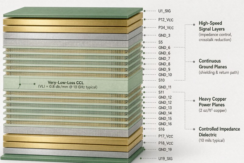
On the board side this pushes two things. First, the power plane structure has to deliver current with acceptable DC drop, which usually means heavier copper and more plane layers than a comparable board would otherwise use. Where the current levels justify it, Heavy Copper PCB construction is worth evaluating early, because it affects layer count, thickness and cost. Second, decoupling has to be placed with an eye on the package’s own inductance rather than on board-level rules of thumb.
The mistake to avoid is treating package decoupling and board decoupling as separate problems. They are one network, and the split between them should be a deliberate decision documented in the design, not a default.
Warpage, CTE and Assembly Reality
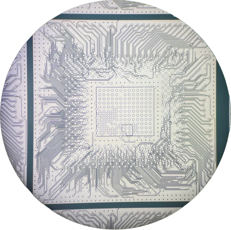
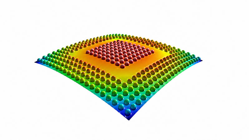
A chiplet package is typically larger and thinner than the monolithic part it replaces, and it is built from materials with different coefficients of thermal expansion. During reflow, that mismatch shows up as warpage, and warpage shows up as non-coplanar balls. The result is open joints at some locations and squeezed joints at others.
Board-level flatness interacts with this directly. A board that is itself not flat, or a pad definition that does not match the package land pattern, compounds the problem. This is where PCB Wire Bonding and other assembly-level capabilities still matter: not every die in a package is flip-chip attached, and where wire-bonded dies or bridge die attach are involved, the assembly house’s process window becomes part of your design constraint.
Assembly yield is also sensitive to how the thermal profile is managed across a large body. Profiles that were acceptable for smaller packages may need to be re-qualified, and that re-qualification is cheaper to do during prototyping than during ramp.
What to Confirm Before You Release
Chiplet designs compress the usual review cycle. Because the package, the substrate and the board constrain each other, decisions that used to be sequential now have to be made together. A short, explicit checklist at the DFM stage prevents most of the expensive surprises:
- Confirm the board fabricator can hold the line/space and microvia structure the escape routing requires, in volume, not just in prototype.
- Confirm ball pitch, land pattern and paste aperture against the package drawing rather than against a previous generation part.
- Agree the stack-up early, including copper weights, and check it against both the impedance targets and the DC drop budget.
- Ask for the package’s coplanarity and reflow flatness specification, and confirm the assembly profile against it.
- Write the via strategy — back-drill, via-in-pad, fill — into the fabrication notes so it is quoted, not assumed.
- Check that the thermal path is defined for each die, not just for the package as a whole.
Theme-wise, the shift is straightforward: chiplet architecture buys system-level flexibility by spending it at the package and board level. Teams that treat the package substrate, the interposer and the PCB as one continuous interconnect problem get the benefit. Teams that treat the board as an afterthought find that the fine-pitch work simply moved downstream, where it is more expensive to fix.
If you are planning a chiplet-based board and want the stack-up, via strategy and material selection reviewed before release, send us the package drawing and the net list. We will come back with a fabrication-feasibility read and the specific items that need a decision.