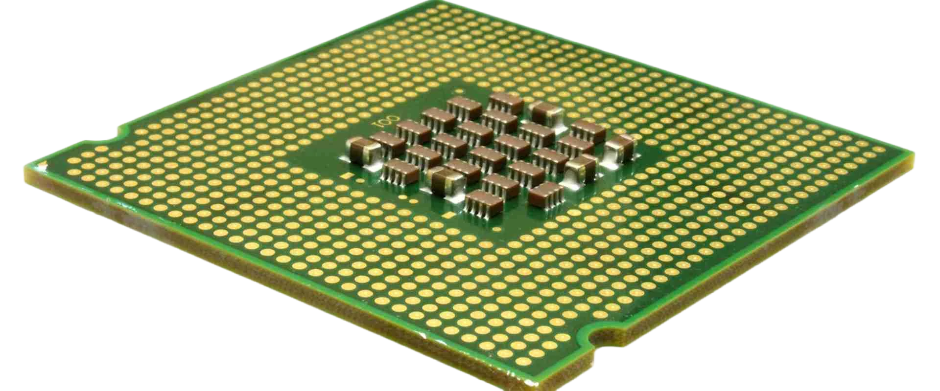
Buyers often treat an IC Substrate as “a PCB, but smaller and more expensive”. The second half of that sentence is true; the first half is where projects go wrong. Substrate-class build is a different manufacturing family with different materials, different via processes, different tolerances and different economics. Knowing where the dividing line sits is what keeps a design from being quoted as substrate when it does not need to be — or quoted as PCB when substrate is the only thing that will work.
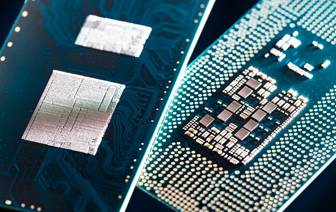
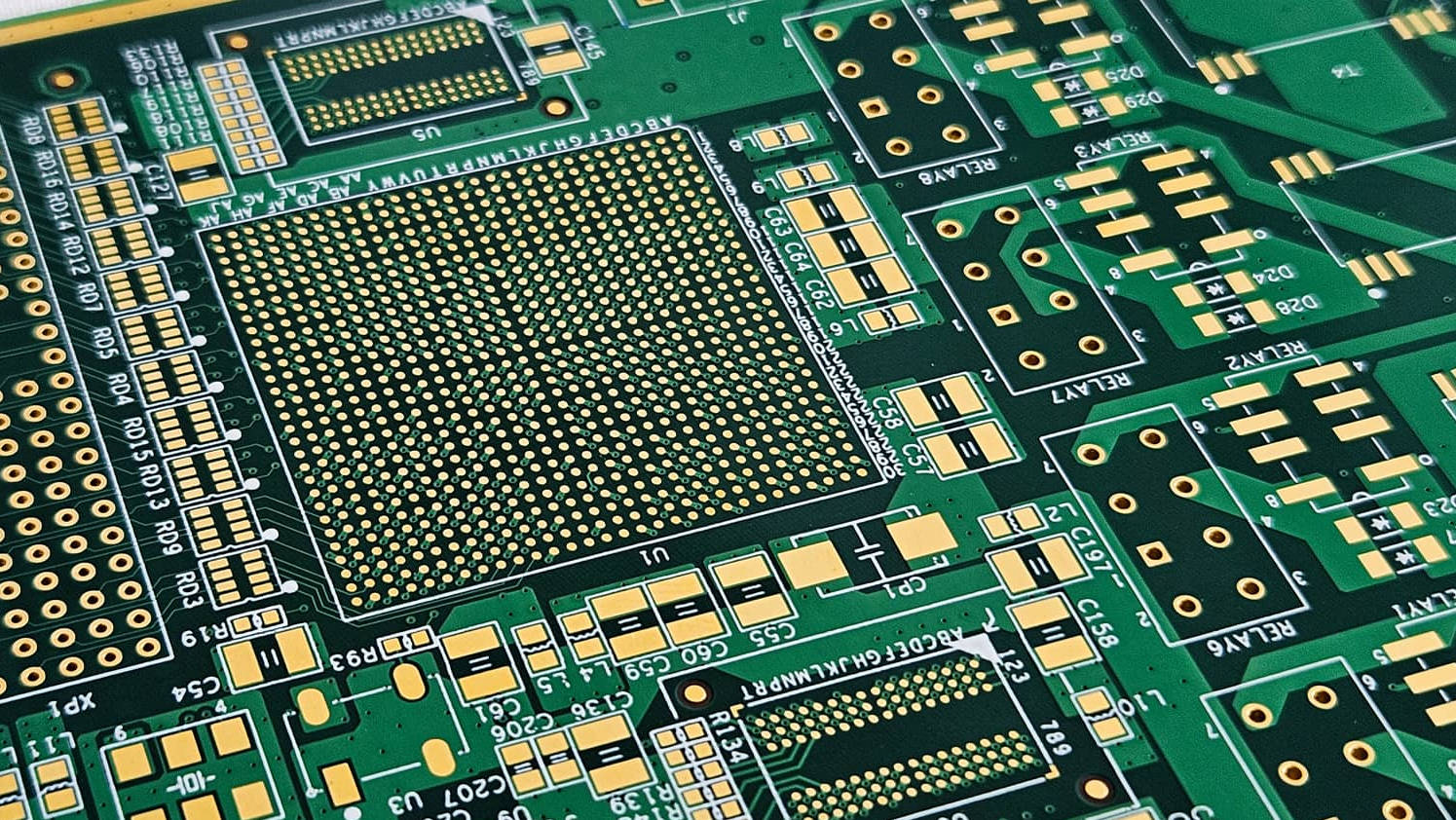
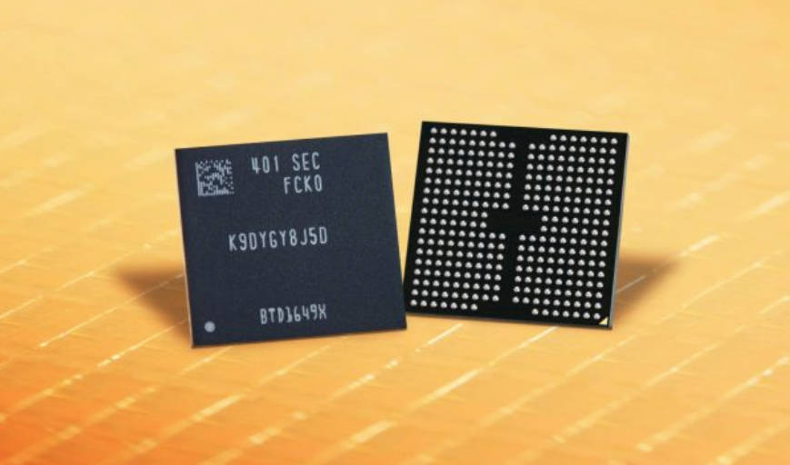
The confusion is understandable. From the outside, a packaged die on a substrate and a large BGA on a board look similar: a flat body with an array of balls underneath. But the layer carrying the fan-out is doing a different job in each case, and it is built by a different process. Once you see which job it is doing, the cost difference stops looking arbitrary.
This article compares the two on the five dimensions that actually change a sourcing decision: feature size, via formation, material systems, dimensional control, and volume economics. It is written for hardware teams and procurement engineers who have to justify the cost difference, not for process engineers running the lines.
The Dividing Line: What Actually Separates the Two
A standard PCB connects packaged components. An IC substrate sits directly beneath a bare die and carries the fan-out from die pads to the package balls. That difference in job description drives everything else.
Because the substrate has to match the die’s pad pitch, its features are much finer than board features. Because it sits directly under silicon, its expansion behaviour has to be managed against the die, not just against the board. And because it is part of the package, its flatness requirement is set by the assembly process rather than by a connector fit.
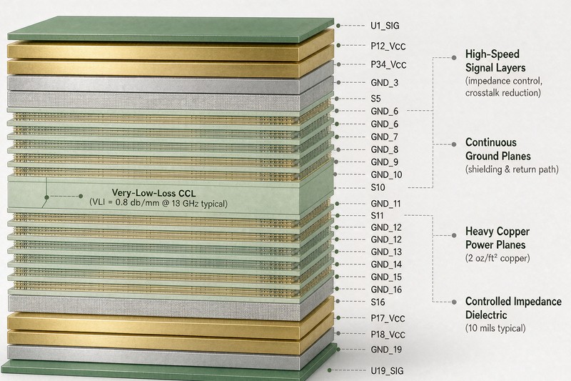
A conventional Multilayer PCB is built by laminating etched copper foils with prepreg and core materials, drilling mechanically or with laser, and plating. Substrate build reverses much of this: layers are built up sequentially on a carrier, vias are formed by laser or photo processes, and the copper is often plated rather than etched away. The equipment, the yield model and the cost structure are all different.
Line and Space: The Capability Gap
Feature size is the cleanest way to see the difference, and the one that most often decides the category. The table below is qualitative — real numbers depend on the supplier, the panel size and the layer count, and must be confirmed against current capability rather than taken from a datasheet of unknown vintage.
| Dimension | Standard PCB | IC substrate |
|---|---|---|
| Typical line/space | Moderate; limited by etch capability | Much finer; limited by build-up process |
| Via formation | Mechanical and laser drilling | Laser and photo-defined microvia |
| Layer build | Laminated core stack | Sequential build-up on carrier |
| Base material | Copper foil, prepreg, core | Build-up film, thin core, copper foil |
| Panel handling | Rigid panel | Thin, often requires carrier support |
| Flatness requirement | Set by assembly fit | Set by die attach and reflow |
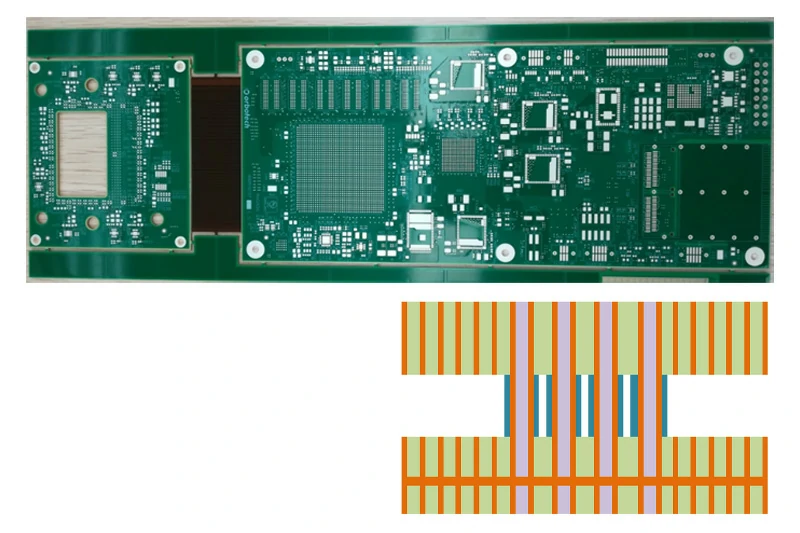
There is a middle ground. Advanced HDI PCB technology borrows several substrate techniques — laser microvias, sequential lamination, thin dielectrics — and applies them at board scale. For many designs that sit between the two categories, high-end HDI is the right answer, and it is usually both cheaper and faster to source than substrate-class build. The mistake is assuming HDI can close a gap it cannot: when the requirement is genuinely set by die pad pitch, no amount of board-level process refinement substitutes for substrate capability.
Via Formation and Layer Build-Up
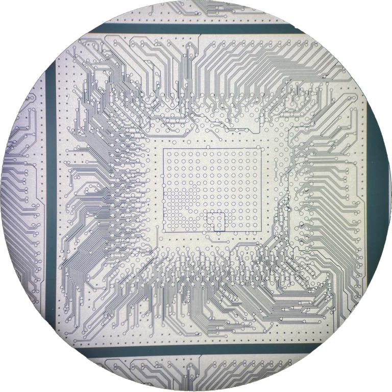
Board vias are drilled. Substrate vias are usually formed by laser ablation or by photo-definition in a dielectric film, then filled and planarised. The difference is not just resolution; it is aspect ratio and shape control. A stacked, filled microvia structure that is routine in substrate build may be at or beyond the edge of what a board shop can produce repeatably in volume.
Sequential build-up also changes the defect model. In a laminated board, most layers are finished before final lamination, and a defect found late usually scraps a panel. In build-up, each added layer is a new yield event, so yield compounds differently and the cost of adding layers rises faster than it does in board construction. That is a real part of why substrate pricing behaves differently as layer count grows.
Material Systems
Boards use copper foil, glass-reinforced prepreg and core materials selected for electrical performance, thermal reliability and process stability. Substrates use build-up films and thin cores chosen for fine-feature resolution, low expansion and compatibility with die attach and reflow. The loss and expansion targets are not the same, and a material that is excellent on one side of the line can be wrong on the other.
Expansion behaviour deserves separate attention. A board is largely designed around its own reliability — thermal cycling, solder joint fatigue, and the expansion of the components mounted on it. A substrate has to manage expansion against silicon, which moves much less. That is why substrate material selection is driven as much by mechanical matching as by electrical performance, and why the thin-core and film constructions used in build-up are not simply thinner versions of board laminates.
For buyers, the practical implication is that material substitution — the usual lever for cost or lead time — is much more constrained on the substrate side. Where a board design might accept several equivalent laminates, a substrate build is often qualified to a specific film system, and changing it means re-qualification rather than a simple swap. If your programme needs second-source flexibility, that needs to be raised during selection, not after qualification. A useful starting point is to review what is documented in the PCB Raw Materials Library and then confirm availability with the supplier for the specific build you are quoting.
Flatness, Warpage and Dimensional Control
Substrate panels are thin and their dimensional stability through reflow is a first-order requirement: die attach and ball attach both depend on it. Board flatness matters too, but it is usually driven by assembly fit and connector mating, which are more forgiving tolerances.
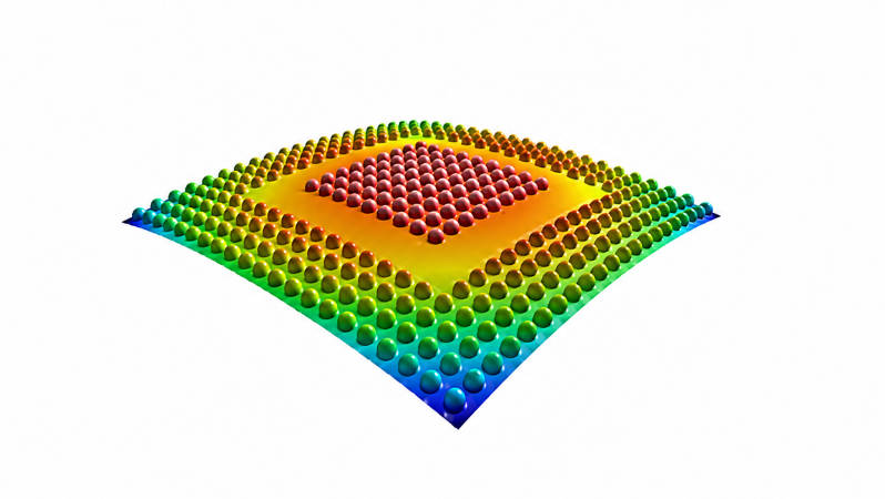
This is why substrate specifications often include coplanarity and warp limits that have no direct analogue in a board drawing, and why those limits have to be measured at temperature rather than at room condition. Measurement method matters as much as the number. A warp figure taken at room temperature on an unmounted part says little about behaviour at reflow, and two suppliers quoting the same nominal limit may not be measuring under comparable conditions. If flatness is a gating requirement for your design, agree the measurement method and the condition before comparing quotes.
If a programme is moving from a packaged part to a bare-die or chiplet approach, the flatness discussion is one of the first things that changes, and it tends to pull the board specification along with it.
Volume Economics and Lead Time
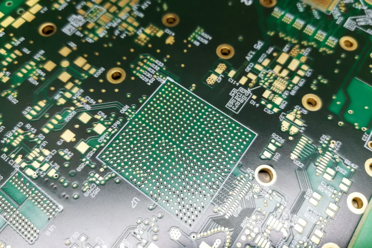
Substrate capacity is concentrated, qualification cycles are long, and tooling and panel utilisation behave differently from board production. In practice this means longer lead times, higher non-recurring costs, and less price elasticity at low volume. It also means the supplier’s willingness to take a prototype depends on whether the build fits their standard process flow — a design that needs a non-standard layer structure or an unusual film will be quoted accordingly.
There is also a scheduling effect. Because substrate capacity is shared across many programmes, a slot that is available in one quarter may not be available in the next, and prototype timing is often gated by capacity rather than by process complexity. Building that uncertainty into the programme timeline is cheaper than discovering it after the board design is frozen.
Before committing to substrate-class build, it is worth confirming what the supplier can actually run at your volume, not just what the capability sheet lists. A review against published PCB Manufacturing Capability and a direct conversation about the specific build will usually surface constraints that a generic capability table hides.
How to Decide: A Practical Checklist
The decision is rarely “substrate or board” in the abstract. It is “which capability does each part of this design actually need”. Working through the following at the DFM review keeps the classification honest:
- Start from the die or fine-pitch component pad pitch. If the fan-out requirement is set by a bare die, substrate-class build is likely unavoidable.
- Check whether advanced HDI can close the gap. If it can, it is usually the cheaper and faster route.
- Separate electrical requirements from geometric ones. A design with modest electrical needs can still be substrate-class purely because of pitch.
- Ask for the flatness and coplanarity limits that apply at reflow, and confirm the board can meet its share of them.
- Confirm material availability and second-source options before qualification, not after.
- Get a volume-dependent quote. Substrate economics change shape between prototype and production more than board pricing does.
The short version: substrate and PCB are not two grades of the same product. They are two manufacturing families that meet in the middle, with high-end HDI bridging part of the distance. Classifying a design correctly at the start is the single cheapest decision in the whole programme.
If you are unsure which side of the line your design falls on, send the pad pitch, layer count and volume. We will tell you which capability it actually needs, and what that means for cost and lead time.