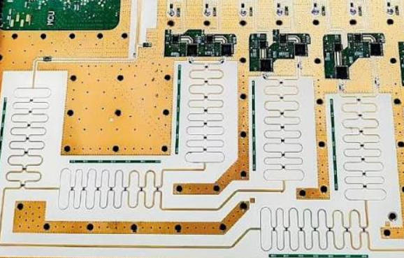
Dielectric constant affects high-frequency PCB performance by changing signal propagation speed, controlled impedance, trace width, wavelength, phase response, and frequency stability. In RF and microwave circuit boards, Dk is not just a material datasheet value. It becomes part of the electrical design.
For standard low-speed PCBs, dielectric constant may not be the first concern. But in high-frequency PCB design, especially for RF modules, radar boards, antennas, microwave circuits, satellite communication equipment, and high-speed transmission lines, Dk can influence whether the fabricated board matches the intended electrical model.
A lower or higher Dk is not automatically better. The correct Dk depends on the operating frequency, impedance target, stackup, trace geometry, antenna size, phase requirement, material tolerance, and fabrication capability.
Mars-PCB supports high-frequency PCB material selection for RF and microwave projects that require material review, stackup planning, and controlled impedance fabrication.
The Short Engineering Answer: What Does Dk Actually Change?
When engineers ask how dielectric constant affects PCB performance, they are usually asking about one of five practical problems:
| Engineering Question | How Dk Is Involved |
| Why does my 50-ohm line width change with material? | Dk affects impedance calculation |
| Why does signal speed change between materials? | Dk changes propagation velocity |
| Why does an antenna shift in frequency? | Dk affects wavelength and resonant dimensions |
| Why does phase matching become unstable? | Dk tolerance and temperature variation affect phase |
| Why does simulation not match fabrication? | Real Dk may differ from assumed Dk or datasheet conditions |
Dk controls how electromagnetic fields interact with the PCB substrate. Once frequency rises, that interaction becomes visible in real circuit behavior.
This is why a high-frequency PCB substrate should be selected together with stackup design, not separately as a purchasing item.
What Is Dielectric Constant in PCB Materials?
Dielectric constant, often written as Dk or Er, describes how a material stores electrical energy in an electromagnetic field compared with air or vacuum. In PCB materials, Dk affects how signals travel through the dielectric between copper layers.
A signal on a PCB trace does not travel only through copper. Its electromagnetic field exists partly in the dielectric material and, depending on the transmission line structure, sometimes partly in air or solder mask. This is why Dk affects signal speed, impedance, wavelength, and RF circuit dimensions.
For PCB design, engineers usually work with an effective dielectric constant rather than only the raw material Dk. The effective value depends on the transmission line type, such as microstrip, stripline, or grounded coplanar waveguide.
| Term | Meaning in PCB Design |
| Dk / Er | Dielectric constant of the PCB material |
| Effective Dk | Apparent Dk experienced by the signal field |
| Design Dk | Practical Dk value used in modeling or impedance design |
| Dk tolerance | Variation range of Dk from material or production |
| Dk stability | How Dk changes with frequency, temperature, or environment |
The important point is that Dk should not be treated as a fixed universal number. A material datasheet may list Dk under a specific test method and frequency, while the final circuit may experience a different effective value after fabrication.
Dk and Signal Propagation Speed
Signal speed in a PCB is slower than in air because the electromagnetic field interacts with the dielectric material. In general, a higher Dk slows the signal more, while a lower Dk allows faster propagation.
This matters in:
- RF transmission lines
- High-speed digital routing
- Differential pairs
- Phase-matched signal paths
- Radar feed networks
- Antenna arrays
- Timing-sensitive communication circuits
Higher Dk generally means slower signal propagation and shorter wavelength inside the PCB material.
For some applications, faster propagation is desirable. For others, controlled delay or compact circuit size may matter more. This is why “lower Dk is always better” is an oversimplification.
In high-speed digital systems, propagation delay affects timing margin. In RF and microwave systems, wavelength and phase behavior may affect matching networks, filters, couplers, resonators, and antenna structures.
Dk and Controlled Impedance
Controlled impedance is one of the most direct ways Dk affects PCB performance. A PCB trace becomes a transmission line when the signal frequency or edge rate is high enough. The characteristic impedance depends on the geometry of the trace and the dielectric environment around it.
Key impedance variables include:
| Variable | Impact on Impedance |
| Dk | Changes field behavior and required trace geometry |
| Dielectric thickness | Sets distance between trace and reference plane |
| Trace width | Main adjustable geometry for impedance |
| Copper thickness | Changes effective conductor shape |
| Solder mask | Can affect outer-layer microstrip impedance |
| Ground plane | Provides reference and return path |
| Trace spacing | Important for differential pairs and coplanar structures |
| Etching tolerance | Changes the final manufactured trace width |
If two PCB materials have different Dk values, the same trace width will not produce the same impedance. For example, a trace designed as 50 ohms on one RF PCB substrate may need a different width on another material.
In controlled impedance PCB design, Dk must be evaluated together with dielectric thickness, copper thickness, trace width, and the actual manufacturable stackup.
This is why engineers should confirm the stackup with the PCB manufacturer before finalizing RF line widths.
Dk and Trace Width Design
Dk affects how wide a trace must be for a target impedance. In many PCB transmission line structures, a higher Dk tends to require a narrower trace for the same impedance and dielectric thickness. A lower Dk may require a wider trace.
This creates a practical layout tradeoff.
| Dk Direction | Possible Layout Effect | Engineering Tradeoff |
| Lower Dk | Wider traces may be needed for the same impedance | Easier fabrication in some cases, but may consume more space |
| Higher Dk | Narrower traces may be possible | Helps compact layout, but may increase fabrication sensitivity |
| Stable Dk | More predictable impedance | Better repeatability between design and production |
| Variable Dk | Impedance may shift | Higher risk for RF and high-speed designs |
For dense RF modules, higher Dk may help reduce circuit size. For some antenna or low-loss routing applications, lower Dk may be preferred. The right Dk depends on whether the design priority is size, loss, impedance tolerance, bandwidth, or manufacturability.
Dk and Wavelength in RF/Microwave Circuits
In high-frequency PCB design, physical dimensions often relate to wavelength. Antennas, filters, resonators, matching networks, and couplers may depend on electrical length. Dk changes the wavelength inside the PCB material.
A higher Dk shortens the wavelength. This can make circuits more compact, but it may also make them more sensitive to tolerance. A small dimensional variation may become more significant when the structure is already small.
A lower Dk provides a longer wavelength inside the material. This can be useful for some low-loss RF paths, but it may increase the physical size of structures.
Where Dk-Related Wavelength Effects Matter
| Circuit Feature | Why Dk Matters |
| PCB antennas | Dk affects resonant dimensions and tuning |
| Filters | Dk affects frequency response and element length |
| Couplers | Dk affects electrical length and coupling behavior |
| Resonators | Dk affects resonant frequency |
| Radar feed networks | Dk affects phase and path matching |
| Microwave interconnects | Dk affects impedance and phase delay |
For RF and microwave PCBs, Dk can shift the relationship between physical length and electrical length.
This is one reason radar, antenna, and microwave circuit boards often require closer material and fabrication control than ordinary PCBs.
Dk Stability: The Part Many Buyers Ignore
A single Dk number is not enough. Engineers also need to know how stable that Dk is.
Dk may vary with:
- Frequency
- Temperature
- Material axis
- Resin and glass composition
- Laminate thickness
- Manufacturing lot
- Moisture absorption
- Fabrication process
- Test method
Rogers technical guidance notes that PCB material Dk values are usually tied to specific test methods and frequencies, and that Dk can change under different conditions. Rogers also notes that many PCB materials are anisotropic, meaning Dk can differ by material direction.
For high-frequency PCB performance, this matters because the board may operate across temperature, frequency range, and production batches.
| Dk Behavior | Possible PCB Impact |
| Dk changes with frequency | Frequency response may shift |
| Dk changes with temperature | Phase and impedance may drift |
| Dk varies by direction | Different field orientations may behave differently |
| Dk tolerance is wide | Board-to-board repeatability may suffer |
| Dk is stable | Easier to maintain predictable RF behavior |
For this reason, high-frequency PCB material selection should consider not only nominal Dk but also Dk tolerance and stability.
Dk Is Not Df: Do Not Confuse Speed with Loss
Dk and Df are often discussed together, but they affect different aspects of PCB performance.
Dk affects signal speed, impedance, wavelength, and geometry. Df, or dissipation factor, affects dielectric loss. A material can have a suitable Dk but still have too much loss for a high-frequency application.
| Parameter | Main Question It Answers |
| Dk | How does the material affect signal speed and geometry? |
| Df | How much signal energy is lost in the dielectric? |
| Copper roughness | How much conductor loss may occur? |
| Thickness tolerance | How stable will impedance be? |
| CTE | How stable is the board under thermal stress? |
In real PCB design, all of these parameters work together. A low Dk material does not automatically mean low loss. A low Df material does not automatically solve impedance problems. The stackup, trace geometry, copper surface, and fabrication process still matter.
Material Selection: Should You Choose Low Dk or High Dk?
The answer depends on the design goal.
| Design Goal | Dk Direction Often Considered | Reason |
| Faster signal propagation | Lower Dk | Lower Dk generally supports faster propagation |
| Smaller RF structures | Higher Dk | Higher Dk shortens wavelength and can reduce size |
| Easier wider impedance traces | Lower Dk in some stackups | Wider traces can be easier to fabricate |
| Compact dense routing | Higher Dk in some cases | Narrower lines may fit tight layouts |
| Antenna tuning stability | Stable Dk | Repeatability matters more than nominal value |
| Phase-sensitive RF paths | Stable Dk and tight tolerance | Phase consistency depends on material behavior |
| Lower insertion loss | Check Df, not only Dk | Df and copper loss are more directly tied to loss |
The key is not to chase the lowest Dk. The key is to select a Dk value that supports the intended circuit geometry and can be manufactured consistently.
How Dk Affects Stackup Evaluation Before Fabrication
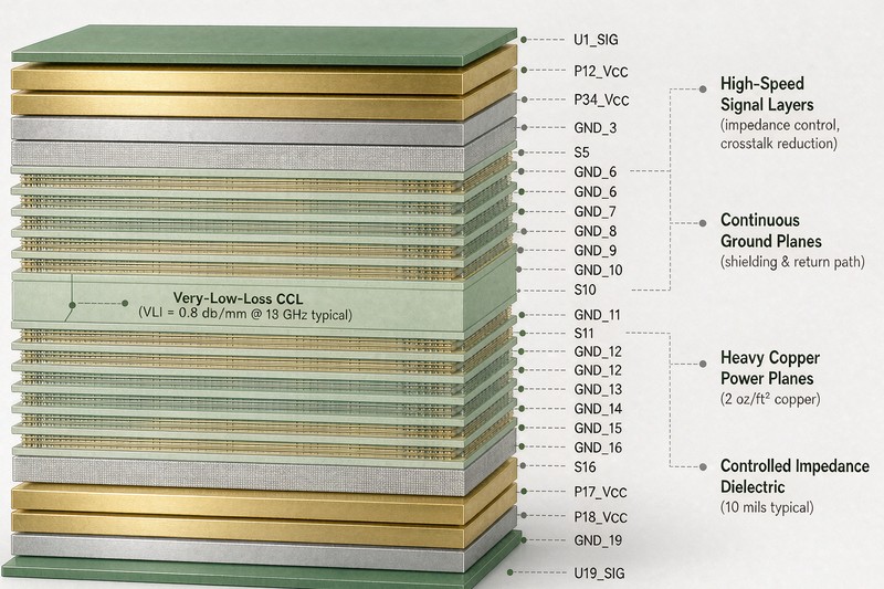
A high-frequency PCB stackup should be reviewed before fabrication because Dk affects the relationship between material, layer spacing, and trace geometry.
A proper stackup discussion should include:
| Stackup Detail | Why It Matters |
| Material grade | Defines nominal Dk and Df |
| Dielectric thickness | Works with Dk to determine impedance |
| Copper thickness | Affects final line geometry |
| RF signal layer | Determines microstrip, stripline, or coplanar structure |
| Ground reference | Controls return path and impedance stability |
| Solder mask condition | May affect outer-layer RF traces |
| Impedance target | Defines required trace width and spacing |
| Dk tolerance | Affects production repeatability |
| Operating frequency | Determines how sensitive the design is to material behavior |
Mars-PCB provides RF PCB substrate and stackup evaluation for high-frequency PCB projects where material choice must match controlled impedance and manufacturing capability.
Practical Example: Same Circuit, Different Dk
Consider a simplified RF design requiring a controlled impedance transmission line. If the engineer changes from one PCB material to another with a different Dk, several design details may need to change:
| Design Item | Possible Change When Dk Changes |
| Trace width | May need recalculation |
| Dielectric thickness | May need adjustment |
| Antenna size | May shift due to wavelength change |
| Phase matching | May need rechecking |
| Simulation model | Must use correct material data |
| Fabrication notes | Must specify material and tolerance |
| Impedance coupon | May need updated geometry |
This is why substituting one PCB material for another should not be treated as a simple purchasing decision. Even if the replacement material is “similar,” the actual Dk, Dk tolerance, thickness, and copper type may change the final RF behavior.
Common Mistakes When Using Dk in High-Frequency PCB Design
Mistake 1: Using Datasheet Dk Without Checking Test Conditions
Dk values may be listed under specific test methods, frequencies, or material directions. The number may not exactly represent the effective Dk in a fabricated circuit. For RF designs, engineers should confirm which Dk value is used in simulation and impedance calculation.
Mistake 2: Treating Dk as a Constant Value
Dk may change with frequency, temperature, direction, and thickness. For demanding RF or microwave circuits, Dk stability and tolerance should be reviewed.
Mistake 3: Choosing Low Dk Without Checking Trace Width
A lower Dk may require wider traces for a target impedance. If the board is compact, wider traces may not fit the layout.
Mistake 4: Choosing High Dk Only for Miniaturization
Higher Dk can reduce structure size, but it may also increase sensitivity to manufacturing tolerance. It may also affect bandwidth or loss depending on the material system.
Mistake 5: Separating Material Selection from Fabrication
A material may look correct in simulation but still be difficult to fabricate in the required thickness, copper weight, or multilayer stackup. Material choice should be confirmed with the PCB manufacturer.
What to Send Your PCB Manufacturer for Dk Review
If you are asking for high-frequency PCB material selection or stackup evaluation, do not only say “we need low Dk material.” Provide enough context for the manufacturer to check the design properly.
| Information to Provide | Why It Helps |
| Operating frequency | Determines material sensitivity and loss concern |
| Target impedance | Needed for trace geometry and stackup calculation |
| Transmission line type | Microstrip, stripline, GCPW, or differential pair |
| Preferred material | Helps quote and verify exact laminate |
| Acceptable alternatives | Allows cost-performance comparison |
| Stackup drawing | Defines layer order and dielectric spacing |
| Copper thickness | Needed for impedance calculation |
| RF-critical areas | Highlights antenna, feed line, or phase-sensitive sections |
| Surface finish | May affect assembly and RF behavior |
| Quantity and project stage | Prototype and production planning may differ |
For RF, microwave, radar, antenna, or high-speed projects, Mars-PCB can support dielectric constant PCB material review before fabrication.
How to Evaluate a PCB Supplier for Dk-Sensitive Projects
A supplier working on Dk-sensitive boards should understand the relationship between material, stackup, impedance, and manufacturing tolerance. The supplier should not only accept a material name and process the order without review.
Ask the supplier:
- Can you confirm the exact material grade and Dk value used for stackup calculation?
- Can you process the required laminate thickness?
- Can you calculate controlled impedance based on the manufacturable stackup?
- Can you identify whether the RF lines are microstrip, stripline, or coplanar waveguide?
- Can you review trace width and spacing tolerance?
- Can you provide impedance test coupons if needed?
- Can you support prototype and production consistency?
- Can you recommend material alternatives if the selected substrate is not practical?
For broader PCB production requirements, engineering teams can also review Mars-PCB custom PCB manufacturing when planning fabrication, assembly, or long-term supply.
FAQ
What is dielectric constant in PCB materials?
Dielectric constant, or Dk, describes how a PCB material affects an electromagnetic field. In PCB design, it influences signal speed, controlled impedance, wavelength, trace geometry, and RF circuit dimensions.
How does dielectric constant affect PCB impedance?
Dk affects how electromagnetic fields travel between a trace and its reference plane. For the same stackup and trace width, a different Dk can produce a different impedance, so RF trace geometry often needs recalculation when material changes.
Is lower Dk better for high-frequency PCB design?
Not always. Lower Dk can support faster signal propagation and may reduce some layout sensitivity, but higher Dk can help reduce circuit size. The right Dk depends on impedance, antenna size, phase behavior, stackup, and fabrication needs.
Why does Dk stability matter in RF PCB substrates?
Dk stability matters because changes in Dk can shift impedance, phase, frequency response, and antenna tuning. RF PCB substrates should be evaluated by Dk tolerance and stability, not only by nominal Dk.
What is the difference between Dk and Df in PCB materials?
Dk affects signal speed, impedance, and wavelength. Df affects dielectric loss. A high-frequency PCB material should be evaluated by both Dk and Df, along with thickness tolerance, copper roughness, and fabrication capability.
Can the same PCB design use a different Dk material?
Sometimes, but the RF traces, impedance, antenna dimensions, and simulation model may need to be recalculated. Substituting material without engineering review can cause performance shifts.
What information is needed for high-frequency PCB material selection?
Engineers should provide operating frequency, target impedance, stackup, transmission line type, material preference, copper thickness, RF-critical areas, surface finish, and project quantity for proper material and Dk review.
Conclusion
Dielectric constant has a direct effect on high-frequency PCB performance. It changes signal speed, impedance, wavelength, phase response, trace geometry, antenna behavior, and frequency stability.
For engineers, the practical lesson is clear: do not choose PCB materials by nominal Dk alone. Review Dk together with Df, dielectric thickness, copper thickness, copper roughness, stackup structure, Dk tolerance, operating frequency, and manufacturing capability.
Mars-PCB supports high-frequency PCB material selection for RF PCB, microwave PCB, radar PCB, antenna PCB, and high-speed circuit board projects that require Dk-sensitive stackup and fabrication review.