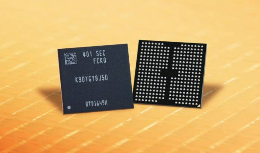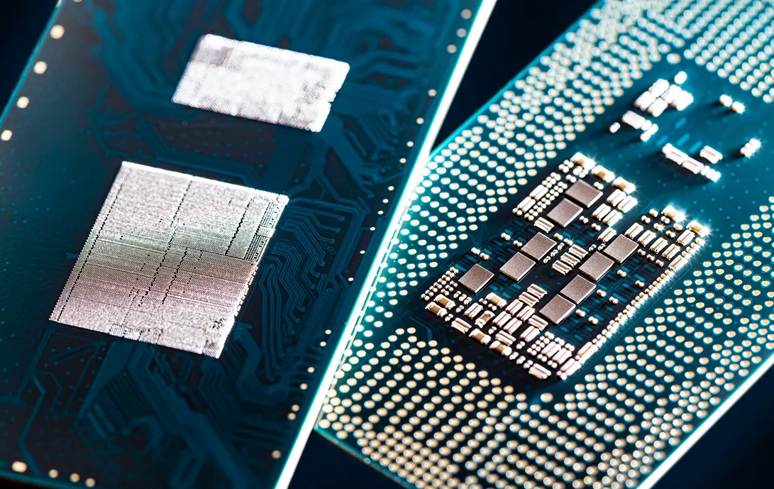
Chiplet-based design replaces one large system-on-chip with several smaller dies that are connected inside a single package. This shift moves the most demanding interconnect work off the motherboard and into the package itself, so the package substrate — not the PCB — now carries the finest lines and the highest wiring density. This article explains how chiplet packaging works in 2.5D and 3D configurations, how substrate requirements change as a result, and what those changes mean for the PCBs and assembly processes that support the final product.
For readers evaluating suppliers, the key decision factors are: which interposer architecture a package uses, how the substrate material and warpage control are specified, and whether the downstream PCB can handle the power delivery and flatness demands of large chiplet packages. Each factor is covered in the sections below.
What Chiplets Are and Why Packaging Is Changing
A chiplet is a small, functional die — a CPU core complex, an I/O controller, a memory controller, or an analog block — that is manufactured separately and then combined with other dies in one package. Instead of monolithic scaling, system designers assemble chips the way system architects assemble boards: from verified building blocks.
The main reasons for this shift are practical. Smaller dies yield better than very large ones, so splitting a big design reduces the cost impact of defects. Different chiplets can be built on different process nodes, letting digital logic use advanced nodes while analog and I/O blocks stay on mature, cheaper processes. Finally, reusing a proven chiplet across products shortens development cycles.
Two packaging styles dominate this approach:
- 2.5D packaging places dies side by side on an interposer — a small, extremely fine-line piece of silicon or organic material — that routes the die-to-die signals and connects down to the package substrate.
- 3D packaging stacks dies on top of each other and connects them vertically, through-trench structures known as through-silicon vias (TSVs), microbumps, or direct copper-to-copper bonding.
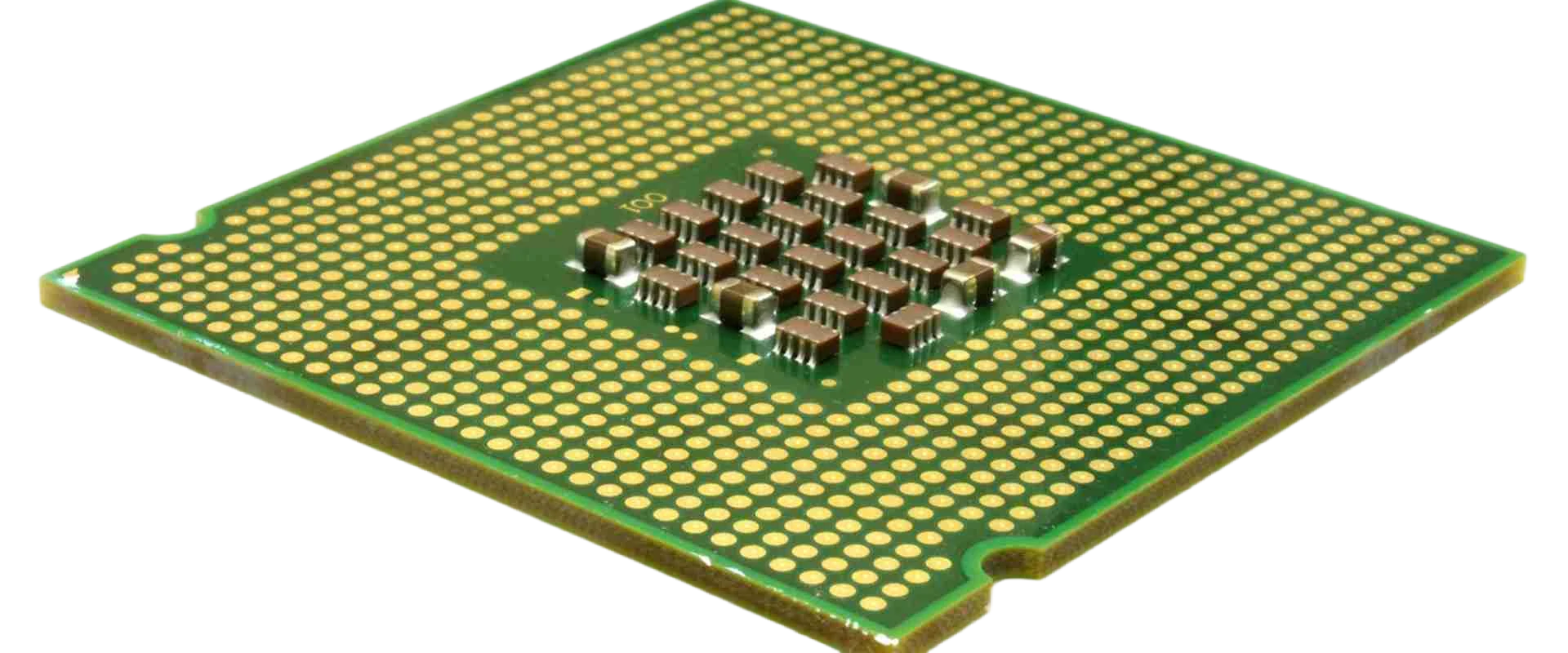
In both styles, the package substrate sits between the interposer or die stack and the outside world, and in both styles the substrate inherits requirements that conventional packages never faced. When the interposer itself is not used, the die attaches directly to a dedicated IC substrate whose wiring density approaches interposer-class levels.
2.5D Packaging: The Interposer Carries the Fine Lines
In a 2.5D package, the silicon interposer is the highest-density wiring layer. Die-to-die signals run through it at line widths and spacings far below what any laminate substrate can reach, with TSVs carrying signals vertically through the interposer thickness. Below the interposer, signals fan out through the package substrate and exit through a BGA ball field.
An organic redistribution layer (RDL) interposer is the common alternative to silicon. It replaces the silicon wafer with buildup layers of fine-line copper wiring, trading some wiring density for lower cost and a CTE closer to the package substrate. The choice between silicon and organic interposers affects what is demanded of the substrate underneath: a silicon interposer presents a severe CTE mismatch that the substrate must absorb, while an organic interposer pushes finer-line requirements closer to the substrate itself.
For buyers, the practical consequence is that substrate selection for 2.5D packages is no longer a secondary decision. The substrate must fan out a very dense ball field, stay flat through reflow, and remain dimensionally stable next to the interposer — all at body sizes that grow with every product generation.
3D Packaging: Stacked Dies Move Interconnects Vertical
3D packaging connects dies vertically. Upper dies communicate with lower dies through TSVs and microbumps, and at the highest integration levels, hybrid bonding joins copper pads directly without solder, removing the bump entirely between stacked dies.
Wire bonding remains relevant in cost-sensitive stacked configurations, where a die is mounted face-up and connected to the substrate by bond wires. Planning for this means accounting for loop height, bond angle clearance, and die-edge keep-out zones early in layout; supplier guidance on PCB wire bonding and die-attach layout typically applies to these hybrid configurations.
The defining constraint of 3D packaging is thermal. Heat generated in stacked dies must travel through the die stack before reaching the substrate, so substrate design directly affects how efficiently heat exits the package. Thicker copper planes, thermal via arrays under the package, and substrate material choice all influence the thermal path — details that must be confirmed with the supplier based on the actual power map of the stack.
How Substrate Requirements Change Under Chiplet Packaging
Chiplet and 2.5D/3D packaging raise the bar for package substrates in four concrete ways:
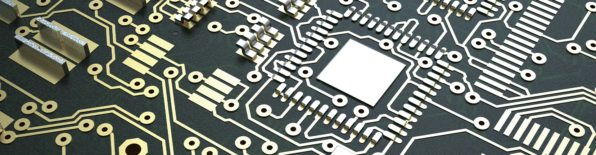
- Wiring density. The substrate must fan out ball fields from interposers and die stacks at finer line widths than conventional packages require. The buildup layers involved sit at density levels normally associated with advanced HDI/ELIC PCB manufacturing rather than standard laminate work.
- Material system. BT resin and ABF (Ajinomoto Build-up Film) dominate package substrates for these architectures because of their dimensional stability and electrical performance at high frequency. ABF is typical for fine-line, high-layer-count substrates under large dies; BT is common where wire-bond or lower-density configurations are acceptable.
- CTE matching. Silicon, the interposer, and the laminate substrate expand at different rates. The substrate’s CTE must be low and closely controlled so that solder joints at the interposer interface stay within fatigue limits over temperature cycling. Exact CTE targets depend on the package construction and should be confirmed with the substrate supplier.
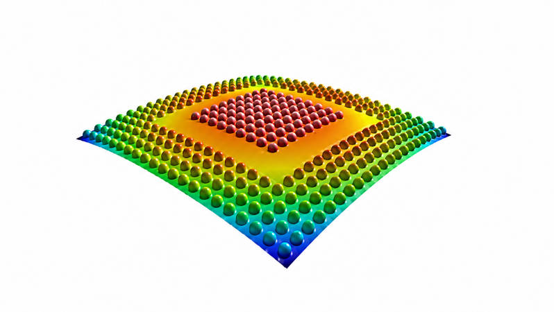
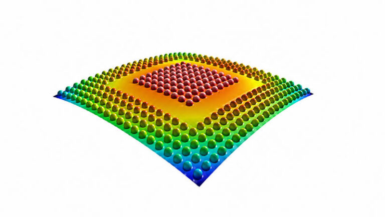
- Warpage control. Large body sizes amplify warp. A substrate that is flat at room temperature can bow at reflow temperatures, causing open joints at the interposer interface or at the BGA balls below. Warpage specifications at both room and reflow temperature are therefore a primary acceptance criterion, not an afterthought.
How Downstream PCB Requirements Shift
One counterintuitive effect of chiplet packaging is that the motherboard itself can become simpler in some respects while becoming more demanding in others.
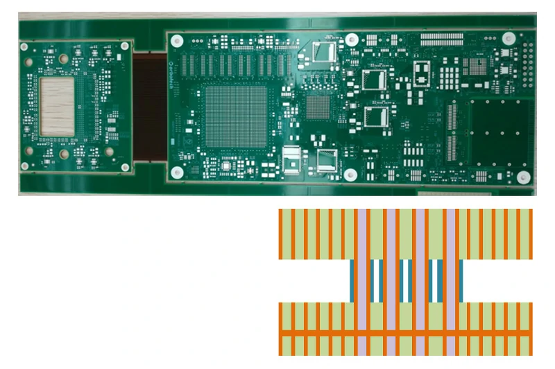
The simplification: die-to-die signals never leave the package, so the board no longer needs to route ultra-fast serializer or memory interfaces between separate chips. Compared with a board carrying multiple discrete high-pin-count devices, a single large chiplet package can reduce the trace density the motherboard needs — conventional multilayer PCB construction often suffices where a denser stack-up would otherwise have been required.
The added demands concentrate in three areas:
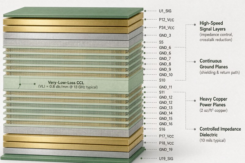
- Power delivery. Chiplet packages concentrate high transient currents in one footprint. The board under the package typically needs more power and ground planes, low-inductance decoupling placement, and — depending on the power budget — heavier copper in the layers serving the package.
- Flatness and support. A large, thin package substrate sitting on a warped board compounds warpage at the second-level BGA interface. Board flatness specifications and package placement zones deserve explicit attention in the stack-up drawing.
- Thermal design. Heat exiting the package enters the board first. Thermal via arrays under the package footprint, plane spreading, and — where the application justifies it — metal-core or embedded-heat-path constructions change how effectively the board moves that heat away.
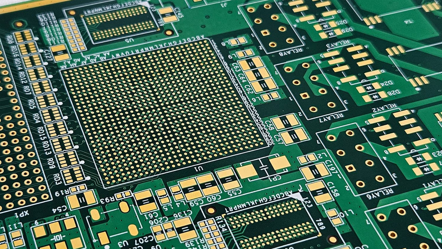
Assembly is the third touchpoint. Chiplet packages arrive as large, fine-pitch BGA components, and mounting them successfully depends on paste printing accuracy, coplanarity checks, and reflow profile control — the same process disciplines that govern demanding BGA assembly work in general, applied at larger body sizes and tighter tolerances.
What Buyers and Designers Should Confirm With Suppliers
Because chiplet packaging distributes technical risk across substrate, package, and board, a structured checklist keeps requirements aligned before ordering:
| Item to Confirm | Why It Matters |
|---|---|
| Substrate material system (BT vs. ABF) and achievable line/space | Determines whether the substrate can fan out the interposer ball field |
| Warpage specification at room and reflow temperature | Largest single risk to assembly yield on large body sizes |
| CTE values of substrate and interposer interface | Governs solder joint fatigue life over temperature cycling |
| Board stack-up: power plane count, copper weight, flatness zones | Power delivery and package flatness depend on it |
| Thermal path design under the package footprint | 3D stacks concentrate heat; the board is the first exit path |
| Assembly process window for large fine-pitch packages | Printing, placement, and reflow tolerances tighten with body size |
A DFM review that includes the package substrate, the interposer choice, and the board stack-up together — rather than reviewing each in isolation — surfaces CTE and warpage conflicts before they reach production.
Conclusion
Chiplet packaging moves the highest-density interconnects from the motherboard into the package, and that relocation rewrites the requirement list at both levels. In 2.5D designs, the silicon or organic interposer carries the fine lines while the substrate must fan out dense ball fields, control CTE mismatch, and stay flat at reflow; in 3D stacks, vertical interconnects make the substrate the main thermal exit path. Package substrates therefore demand buildup wiring density, BT or ABF material systems, and explicit warpage acceptance criteria. Downstream, the motherboard often needs less routing density but more power planes, heavier copper where the power budget requires it, tighter flatness control, and deliberate thermal design under the package. Buyers who confirm substrate material, warpage specs, CTE values, board stack-up, thermal path, and assembly process windows early — ideally in a combined DFM review — avoid the conflicts that surface too late in chiplet-based products.
If you are planning a chiplet-based or 2.5D/3D packaged product, share your package outline, die stack description, power budget, and target operating environment with the engineering team to review substrate and PCB requirements together before committing to a stack-up.
FAQ
What is the difference between 2.5D and 3D packaging?
In 2.5D packaging, dies sit side by side on an interposer that routes die-to-die signals horizontally. In 3D packaging, dies are stacked vertically and connected through TSVs, microbumps, or hybrid bonding. 2.5D emphasizes interconnect density between dies; 3D adds vertical integration and makes heat extraction the primary design constraint.
Why does chiplet packaging raise substrate requirements?
Because the package substrate must now fan out very dense ball fields from the interposer or die stack, absorb CTE mismatch between silicon and laminate, and stay flat through reflow at large body sizes. These requirements push substrate wiring density and material specifications above conventional package levels.
Does chiplet packaging make the PCB simpler?
Partly. Die-to-die signals stay inside the package, so the motherboard often needs less trace density than a discrete-chip design. However, the board needs more power and ground planes for high transient currents, tighter flatness under large packages, and a designed thermal path to remove heat exiting the stack.
Which assembly issues matter most for large chiplet packages?
Warpage at reflow, substrate and board coplanarity, paste printing accuracy for fine-pitch BGA fields, and reflow profile control. These are extensions of standard demanding BGA process control, applied at larger body sizes where small deflections cause open joints.