Embedded passives in PCB design make sense when board area, electrical performance, or assembly yield matter more than the added process cost. They are usually justified in dense, high-frequency, or height-constrained designs where a capacitor or resistor has to sit closer to the load than any surface-mounted part allows. They are usually the wrong choice when the design still changes late, the value range is wide, or the volume is too low to absorb the extra process steps.
This article explains what counts as an embedded component, where embedding pay-offs are real, how resistors and capacitance are actually built into a board, which design rules decide the outcome, and when discrete parts remain the better answer.
What Counts as an Embedded Component
The term covers several different constructions, and mixing them up is the most common source of wrong cost expectations.
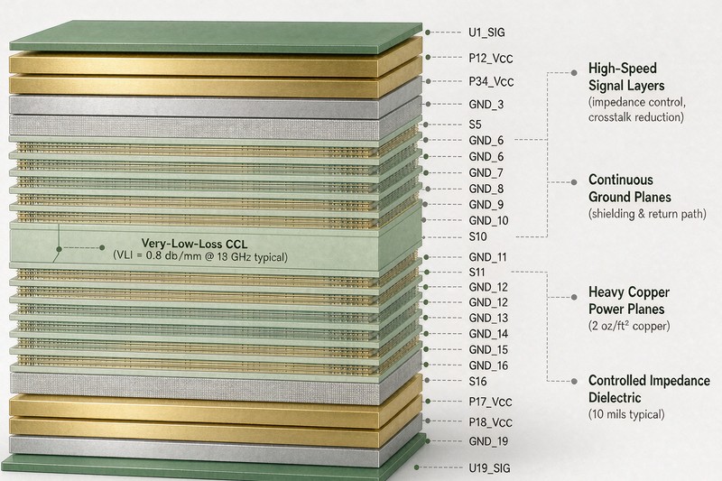
- Formed-in-layer passives — a resistive or capacitive element is created inside the board stackup itself. A resistive foil or printed polymer film is patterned on an inner layer to create resistors; a very thin dielectric between two copper planes creates distributed capacitance.
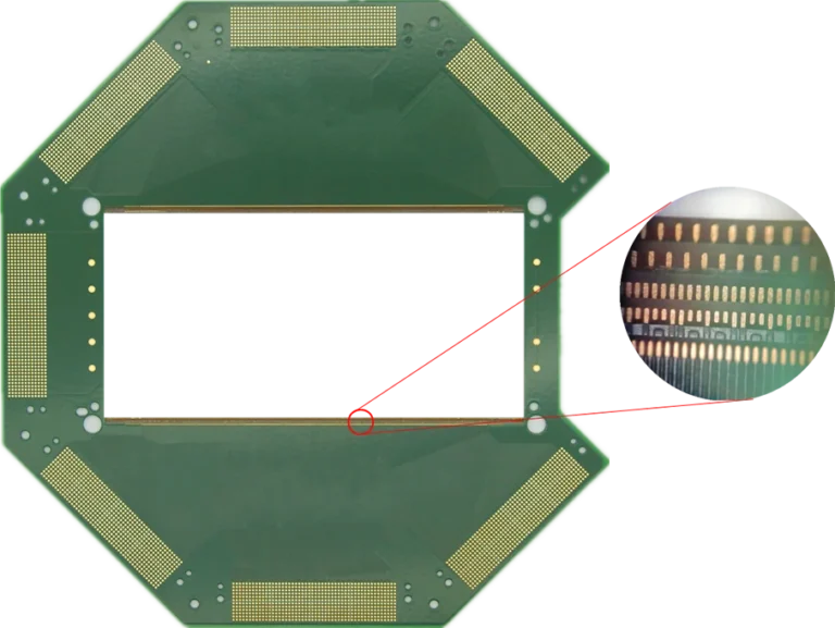
- Discrete components in a cavity — a recess is machined into the board, a standard packaged part (most often a capacitor or a bare die) is placed into it, and the part is interconnected at the cavity level.
- Embedded actives — a packaged device or bare die buried in the build-up. This is a much more specialised process with tighter thermal and test constraints than passive embedding.
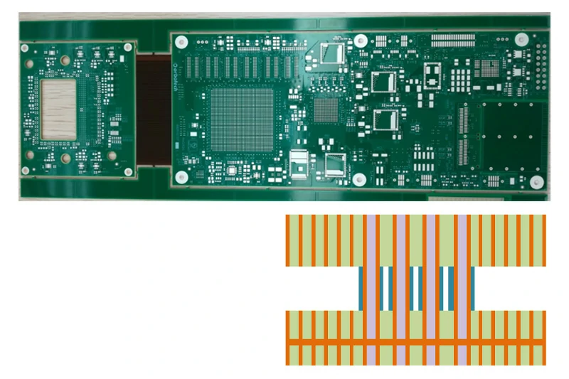
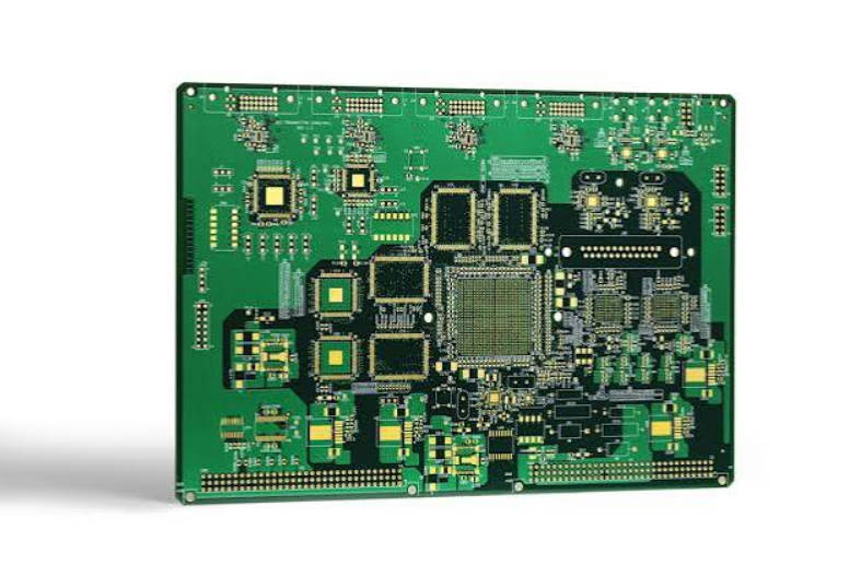
In practice, most commercial designs use the first two. A high-density HDI PCB build-up is the usual host structure, because the fine-line layers and thin dielectrics that make embedding useful are the same features that define HDI.
Where Embedding Passives Pays Off
Four conditions usually drive the decision, and they tend to appear together.
Decoupling distance
A decoupling capacitor works through the loop between the die, the package, and the board. Shortening that loop reduces the inductance the transient current sees. Moving capacitance from the board surface into the package-adjacent layers, or using distributed plane capacitance directly under the device, changes the loop geometry in a way surface placement cannot. This is the strongest technical argument for embedded capacitance.
Surface area pressure
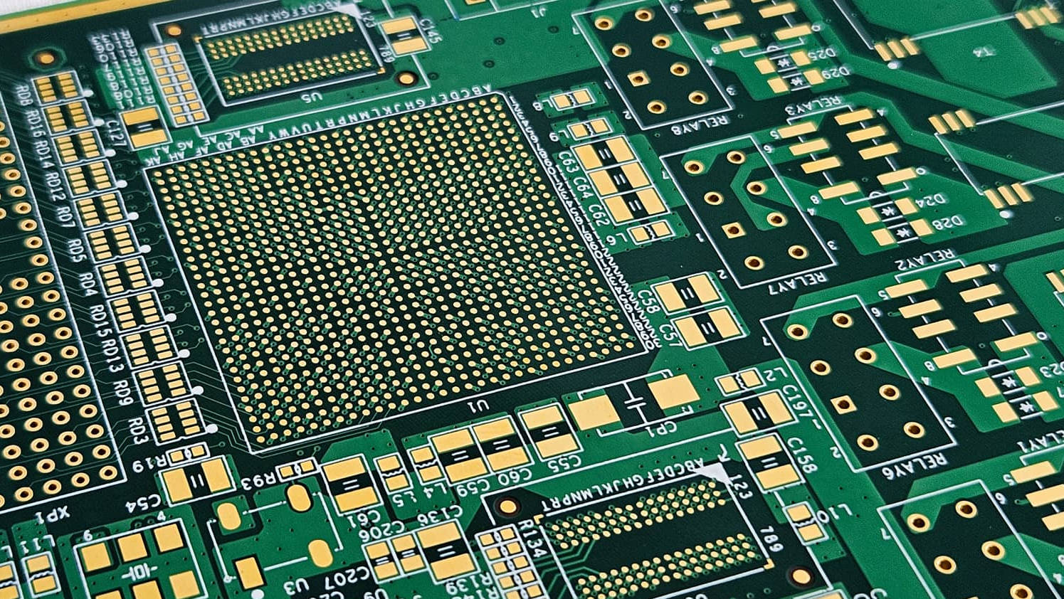
On a dense board, hundreds of 0402 or 0201 decoupling parts consume area that routing also needs, and they force via placement that breaks up reference planes. Moving some of that population inside the board frees surface area for routing and for taller components.
Height and profile limits
Wearable, medical, and handheld products often have a hard Z-height budget. A cavity-mounted part can bring the tallest component below the surface plane.
Assembly and reliability
Fewer solder joints means fewer potential defect sites, and no tombstoning or solder bridging on the parts that move inside. For designs that already run near the limit of placement capability, removing part of the passive population can improve first-pass yield.
These benefits are real but conditional. Whether they outweigh the added process cost depends on the numbers in the next two sections, and a PCB Design review at the concept stage is the cheapest place to test that.
Embedded vs Discrete Passives: What Changes
| Factor | Embedded passive | Discrete passive |
|---|---|---|
| Placement | Inside the stackup or in a cavity | On the surface |
| Board area used | Little or no surface area | Surface area plus keep-out |
| Loop inductance | Lower, depends on layer distance | Higher, set by part and via geometry |
| Value tolerance | Wider as fabricated; can be trimmed | Tight, selected by part code |
| Value changes late | Difficult or impossible after lamination | Simple part swap |
| Rework | Not practical on formed elements | Standard rework |
| Power handling | Limited by heat path through dielectric | Set by the component rating |
| Cost structure | Higher board cost, fewer placements | Lower board cost, more placements |
The decisive rows are usually tolerance, changeability, and cost structure. A design that is still moving will pay for embedding several times over in respins.
Process Routes for Embedded Resistors and Capacitance
Embedded resistors
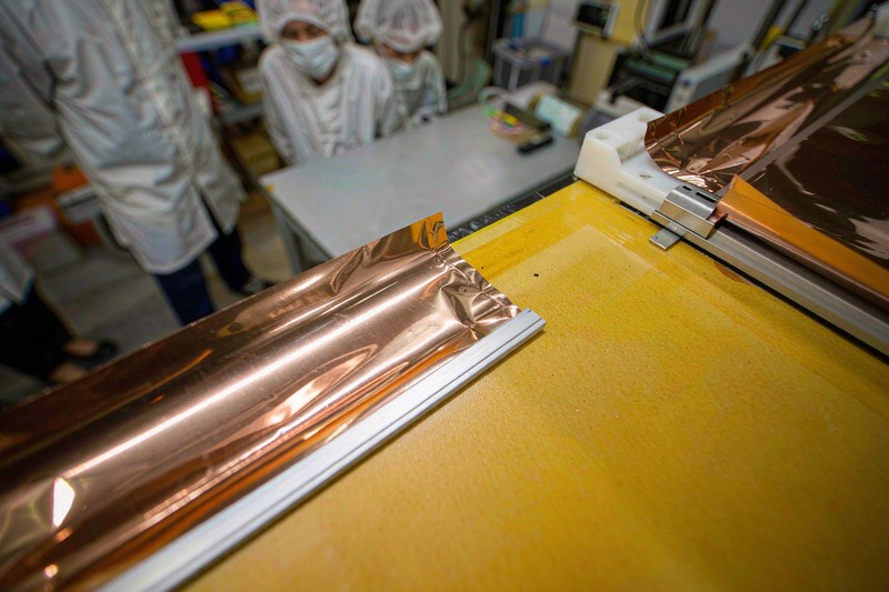
A resistive material — a thin metal alloy film or a screen-printed polymer thick film — is applied to a copper layer, then patterned and etched so that only the resistor bodies remain. The resulting value is set by the sheet resistance of the material and by the length-to-width ratio of the patterned element.
As fabricated, tolerance is typically wider than a discrete part of the same nominal value; laser trimming after formation can tighten it substantially, depending on the process configuration. Trimming needs physical access to the element, so the layer is usually trimmed before final lamination. This constrains stackup order and the point at which the value becomes fixed.
Embedded capacitance
The common approach is distributed capacitance: a power plane and a ground plane separated by a thin dielectric. The capacitance depends on the dielectric constant, the dielectric thickness, and the overlapping area, so thinner dielectric gives more capacitance per unit area.
The practical limits are dielectric thickness tolerance, the voltage rating of the thin layer, and the ability of the laminate to survive lamination and reflow without defects. Exact achievable values should be confirmed with the supplier against the specific material and construction.
Cavity-mounted discretes
A cavity is routed or laser-ablated to a controlled depth, the component is placed and attached inside it, and the cavity is then covered by subsequent lamination or left open depending on the design. Depth control, adhesion inside the cavity, and the interconnect method are the three process risks.
All three routes add steps to an otherwise standard Multilayer PCB sequence, which is why lead time and supplier capability matter as much as the electrical argument.
Design Rules That Decide Whether It Works
Most embedded-passive failures are design-side rather than process-side. These are the items that most often decide the outcome:
- Available values. Sheet-resistance options and achievable resistor geometry define a value window. Values outside it are not available regardless of the layout.
- Power and thermal path. A resistor buried in the stackup dissipates heat through the surrounding dielectric. Derating is essential, and local heating can affect neighbouring circuitry.
- Trim access and timing. If a value must be trimmed, the design has to preserve access at the right process stage and freeze the value before lamination.
- Testability. Formed elements generally cannot be probed after lamination. Test strategy has to be defined before the stackup is frozen.
- Tolerance stack-up. Where several embedded elements set a timing constant, filter corner, or bias point, the combined tolerance must be checked, not the individual one.
- Cavity geometry. Cavity depth, wall clearance, and the cover-layer process interact with component height and placement accuracy.
- Repair expectations. If the product needs field repair of the passive network, embedding removes that option.
These constraints belong in the DFM review, not in a late layout check. A board that needs a cavity and a trimmed resistor layer is also a strong candidate for dedicated Cavity PCBs process review, because the depth-control and lamination requirements overlap.
Cost, Lead Time and Supply Realities
Embedding adds material, imaging, and often trimming steps, and it removes placement operations. The net cost depends on volume, on how many parts move inside, and on how much board area is recovered. The trade usually becomes favourable when either the volume is high enough to amortise the process, or the design has a performance constraint that discrete parts cannot meet.
Lead time is affected in two ways: the process sequence is longer, and the number of suppliers able to run it is smaller. Qualifying the process on a prototype build before committing production volume is normal practice.
Supplier selection should be based on demonstrated capability with the specific construction — resistive foil versus printed film, distributed capacitance versus cavity — rather than on a general capability list. Confirming this against a documented PCB Manufacturing Capability statement, including which constructions are run in-house, is the fastest filter.
When Discrete Passives Still Win
Discrete parts remain the better answer in these situations:
- Design not frozen. Values will change; respins are more expensive than part swaps.
- Wide or unusual value range. Especially high-precision ratios or large capacitance values.
- Low volume. Process setup cannot be amortised.
- High power dissipation. Heat needs an external path.
- Field service required. Repairs must be possible.
- Tight tolerance without trimming. Discrete part codes deliver tolerance directly.
A useful test: if the design can meet its electrical target with parts already on the bill of materials, and board area is not the binding constraint, embedding is usually a cost increase with no performance return.
FAQ
Are embedded passives the same as buried vias?
No. Buried vias are interconnections between inner layers; embedded passives are circuit elements with resistance or capacitance created inside the board. They can coexist in the same stackup and are independent decisions.
Can embedded resistors be trimmed to tight tolerance?
Laser trimming can tighten the value substantially compared with the as-fabricated state, depending on the process configuration. Trimming requires access to the element, so it happens before final lamination and fixes the value early in the build.
Does embedded capacitance replace all decoupling capacitors?
No. Distributed plane capacitance changes the high-frequency part of the decoupling behaviour but does not provide large bulk capacitance. Bulk capacitors normally remain on the surface.
Is a cavity the only way to embed a component?
No. Resistors and capacitance can be formed in the layer stack without any cavity. A cavity is used when a discrete packaged part or a die has to be physically recessed below the surface.
Does embedding improve reliability?
It removes the solder joints of the parts that move inside, which removes those defect sites. It also adds process steps inside the board, so the net effect depends on how well those steps are controlled.
Conclusion
Embedded passives are a stackup decision, not a component substitution. The technical case rests on decoupling loop geometry, surface area recovery, and Z-height — the strongest and most defensible of these is shortening the decoupling loop, because no surface placement can reproduce it. The commercial case rests on volume: the process adds material, imaging, and often trimming steps while removing placement operations, so it pays off when volume amortises the setup or when performance cannot be met any other way.
The decision usually turns on three practical constraints rather than on the electrical argument. Value availability sets a hard window on what can be built. Tolerance and trim timing determine when the design must freeze. Power dissipation and repair access determine whether embedding is viable at all. A design that is still changing, needs unusual values, dissipates meaningful power, or must be serviced in the field should stay with discrete parts.
Before committing, confirm three things with the fabricator: which construction they actually run (resistive foil, printed film, distributed capacitance, or cavity), what tolerance is achievable before and after trimming, and what the process does to lead time. Those three answers settle most embedded-passive decisions.
Share your stackup target, value list, tolerance requirements, and expected volume, and we will confirm which embedded construction fits and what it does to cost and lead time.