Copper pillar bumping and wire bonding place conflicting demands on the same substrate pad frame. Copper pillar asks for fine pitch, tight coplanarity, and filled via-in-pad structures; wire bonding asks for a bondable metallization, generous capillary clearance, and pad geometry that survives thermosonic bonding. When a substrate has to support both — or when the interconnect choice is still open — the pad finish, pad size, via treatment, and keep-out rules must be settled before tape-out, not after.
This article sets out what each interconnect needs, where the two conflict, how to choose pad metallization, and what to confirm with the substrate supplier before release.
Two Interconnect Paths, One Substrate
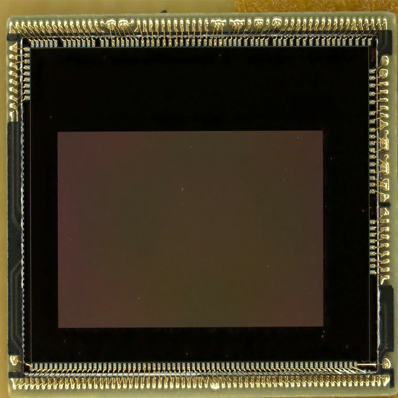
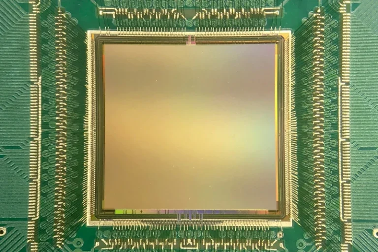
Flip-chip with copper pillar bumps connects the die face-down: an electroplated copper pillar with a solder cap bonds directly to the substrate pad. Wire bonding connects face-up: a fine metal wire is welded from the die pad to a substrate bond pad.
Copper pillar supports finer bump pitch and shorter vertical interconnect than a conventional solder ball, which is why it is the common choice where I/O count is high or electrical and thermal performance at the die interface matters. Wire bonding remains widely used because the process is flexible, the tooling cost is lower, and design changes are easier to absorb.
Both land on the substrate built by the same lamination and imaging sequence. An IC Substrate designed for one can be difficult to convert to the other, because the pad finish and pad geometry decisions are made early in the build.

What Copper Pillar Bumping Demands From the Substrate
Pad pitch and pad size
Bump pitch drives everything downstream. As pitch shrinks, pad diameter shrinks with it, and the routing that escapes the pad array has to fit between pads. This is where fine-line capability becomes the binding constraint rather than the bumping process itself.
Coplanarity and surface condition
Pillar height variation across the die footprint translates into non-uniform standoff after reflow. Pad surface flatness and the planarity of the pad array both matter, and the tolerance tightens as pitch decreases.
Via treatment under the pad
Fine-pitch arrays usually require vias in the pads. An open via under a bump pad creates a solder-void risk and an unreliable interface, so via-in-pad structures are normally filled and planarized before the pad finish is applied.
Alignment and inspection
Fine-pitch assembly needs fiducials and pad definitions that placement and inspection equipment can resolve. The substrate documentation should state what alignment features are included.
What Wire Bonding Demands From the Same Pad Frame
Bondable metallization
Thermosonic bonding works only on a surface that forms a reliable weld with the wire material. A pad that is fine for soldering may not be bondable, and a pad optimized for solderability may have a hard or contaminated surface that prevents wire adhesion. This is the single most common conflict between the two paths.
Pad size and pitch
The bonding capillary has physical width, and the bond cycle needs clearance around the pad. Bond pad pitch is therefore limited by tooling, not only by lithography, and wire length and loop height add further limits on where a pad can sit relative to the die.
Loop height and keep-out
Wires rise above the die surface before coming down to the substrate. Anything placed in the loop path — tall components, cavity walls, stiffeners, or lid features — becomes a clearance problem, and encapsulation or moulding has to accommodate the highest loop.
Pad integrity
Bonding applies force and ultrasonic energy to the pad. Pad adhesion, underlying copper thickness, and any via structure beneath the pad all affect whether the pad survives the cycle without lifting or cracking.
Where a board-level design carries bond pads rather than a package substrate, the same rules apply, and a dedicated PCB Wire Bonding process review is the right place to settle pad finish and pad geometry.
Where the Two Conflict
| Requirement | Copper pillar (flip-chip) | Wire bonding |
|---|---|---|
| Pad pitch | Driven by bump pitch, very fine | Driven by capillary clearance |
| Pad surface | Solderable, planar | Bondable weld surface |
| Via under pad | Filled and planarized | Pad must survive bonding force |
| Vertical space | Die standoff only | Die plus loop height |
| Assembly order | Bump, then attach | Attach die, then bond |
| Change tolerance | Pad frame fixed early | Bond program can adapt |
The surface-finish conflict is the one that causes the most respins. A finish chosen for fine-pitch solder attachment may not accept a wire bond, and a finish chosen for bonding may have different solder behaviour. If a design may use either path, the finish has to satisfy both, and that choice should be confirmed with the supplier against the actual bonding and reflow conditions.
Pad Metallization and Surface Finish Choices
Finish selection should be driven by the interconnect, the wire material, and the assembly thermal profile. The comparison below is directional; exact behaviour depends on the process configuration and should be confirmed with the supplier.
| Finish | Typical strength | Main watch point |
|---|---|---|
| ENIG (electroless nickel, immersion gold) | Flat, solderable, widely available | Nickel layer integrity; bondability depends on wire and conditions |
| ENEPIG (nickel, palladium, gold) | Used where both soldering and bonding are needed | Palladium thickness control |
| Soft / thick gold over nickel | Well established for gold wire bonding | Cost; suitability for fine-pitch solder attachment must be checked |
| OSP | Low cost, flat | Not a wire-bondable surface |
Two practical rules follow. First, do not assume a solderable finish is bondable — confirm it against the specific wire material and bonding parameters. Second, treat finish thickness and underlying nickel condition as controlled parameters, because both affect weld quality and long-term joint reliability.
Design and Process Checks Before Tape-Out
Run these against the release package, whether the design is flip-chip, wire bond, or dual-path:
- Pad finish versus interconnect. Confirm the specified finish is accepted for the actual bonding or bumping process.
- Pad size and pitch versus tooling. Bond pads against capillary geometry; bump pads against placement accuracy.
- Via-in-pad treatment. Confirm fill and planarization method, and whether it is compatible with the finish and the assembly thermal profile.
- Coplanarity target. State the requirement and how it is measured.
- Warpage at assembly temperature. Flatness at room temperature does not predict flatness at reflow.
- Loop clearance and keep-out. For wire bond, check the three-dimensional envelope, not just the footprint.
- Test and inspection access. Confirm pads or fiducials needed for electrical test survive the finish and cover-layer decisions.
- Contamination control. Bonding is sensitive to surface condition; packaging, handling, and storage rules matter.
Items one to four are the ones most often left implicit, and they are also the ones that block conversion between interconnect types later. A DFM pass on the pad frame, plus a material check against the PCB Raw Materials Library for the laminate and finish system, catches most of them before tooling.
How to Specify It in an RFQ
Suppliers can only quote what is written down. The information that changes a quotation on a substrate for either interconnect:
- Interconnect type, and whether dual-path capability is required
- Bump or bond pad pitch, pad diameter, and pad finish
- Via-in-pad requirement and the expected fill and planarization method
- Die size, thickness, and expected standoff or loop height
- Assembly thermal profile, including peak temperature and number of excursions
- Coplanarity and warpage requirements, with measurement method
- Volume and panel utilization expectations
Missing finish and via-treatment information is the most common cause of a quote that later changes. Where the build also involves fine-line build-up layers, confirming them against documented HDI PCB capability avoids quoting a structure that has to be re-engineered.
FAQ
Can one substrate support both copper pillar and wire bonding?
Yes, if the pad frame is designed for it from the start. The binding constraint is the pad finish: it has to satisfy the solder attachment of the pillar and the weld requirements of the wire. Confirm the finish against both processes rather than assuming compatibility.
Why is via-in-pad treated differently for the two paths?
For copper pillar, an open via under a pad creates voiding and standoff variation, so the via is normally filled and planarized. For wire bonding, the concern is different: the pad must withstand the bonding force and ultrasonic energy, so the structure beneath the pad has to remain sound.
Is ENIG always acceptable for wire bonding?
Not always. Bondability depends on the wire material, the bonding parameters, and the condition of the nickel layer. It should be confirmed with the supplier for the specific combination rather than assumed.
What limits wire bond pad pitch?
Capillary geometry and clearance, not lithography. The tool needs room around the pad for the bond cycle, and loop height and wire length add further placement limits.
Does warpage matter differently for flip-chip?
Yes. Flip-chip attachment depends on all pillars making contact within a small standoff window, so substrate flatness at the attachment temperature is critical. Wire bonding is generally more forgiving of substrate shape but adds its own vertical clearance requirement.
Conclusion
Copper pillar and wire bonding are not interchangeable options on the same pad frame. Copper pillar pushes the substrate toward fine pad pitch, filled and planarized vias, and tight coplanarity at the attachment temperature. Wire bonding pushes it toward a bondable metallization, capillary-driven pad pitch and clearance, and a three-dimensional loop envelope that has to be kept clear.
The conflict concentrates in three places. Pad finish is the sharpest: a surface chosen for solder attachment may not form a reliable weld, and a surface chosen for bonding may behave differently in reflow. Via treatment differs in intent — planarization for pillar standoff versus structural integrity under bonding force. Vertical budget differs in kind — die standoff for flip-chip versus die plus loop height for bonding.
That makes the pad frame a tape-out decision. Pad size, pitch, finish, via treatment, coplanarity target, and warpage at assembly temperature have to be written into the release package and confirmed with the fabricator, because these are the items that determine whether the substrate can be converted later. When submitting an RFQ, state the interconnect type, whether dual-path capability is needed, the pad geometry and finish, the via-in-pad method, the thermal profile, and the flatness requirement — those seven items are what make a quotation hold.
Send us your die size, pad pitch, target interconnect, and assembly thermal profile, and we will confirm the pad frame, via treatment, and finish that fit your build.