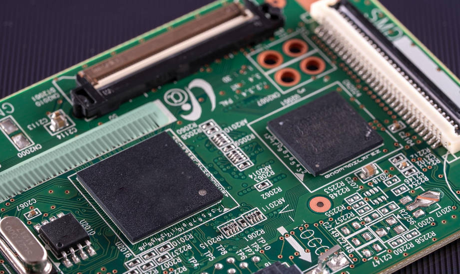
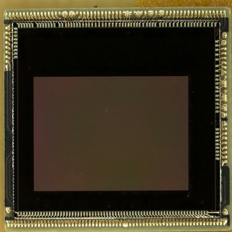
Copper pillar and wire bonding place conflicting demands on one substrate pad frame: pad finish, via treatment, pitch limits and RFQ items to confirm.
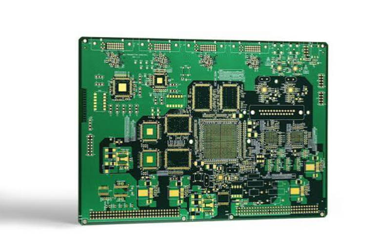
Embedded passives in PCB design pay off when decoupling distance, board area or Z-height is the constraint. Process routes, tolerance and cost trade-offs.
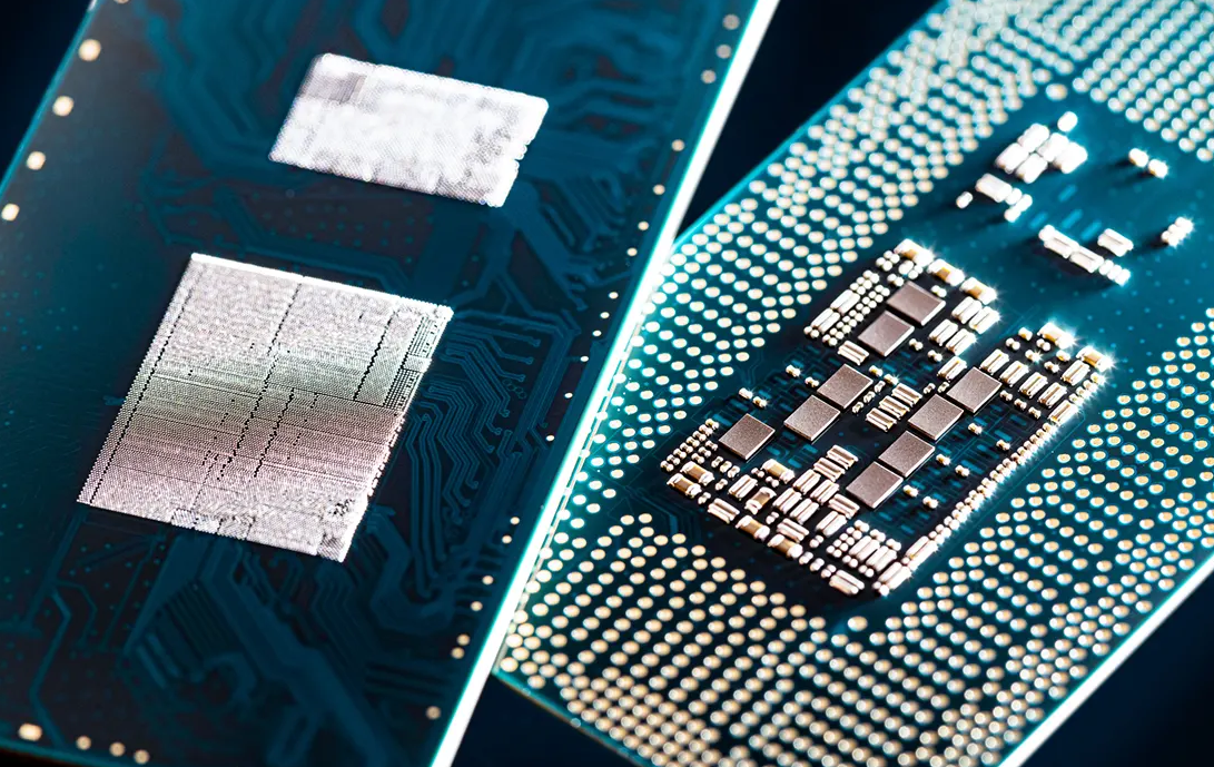
See how chiplet and 2.5D/3D packaging change substrate and PCB requirements, from silicon interposers and RDL layers to CTE matching and warpage control.
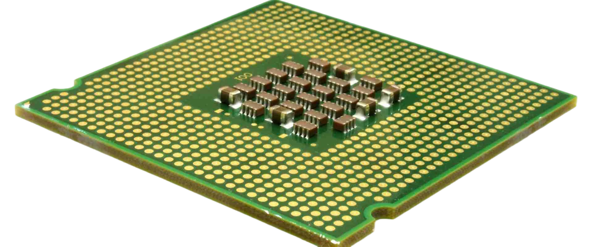
Compare IC substrate and standard PCB capability: feature size, via formation, material systems, flatness and volume economics, plus how to classify a design.
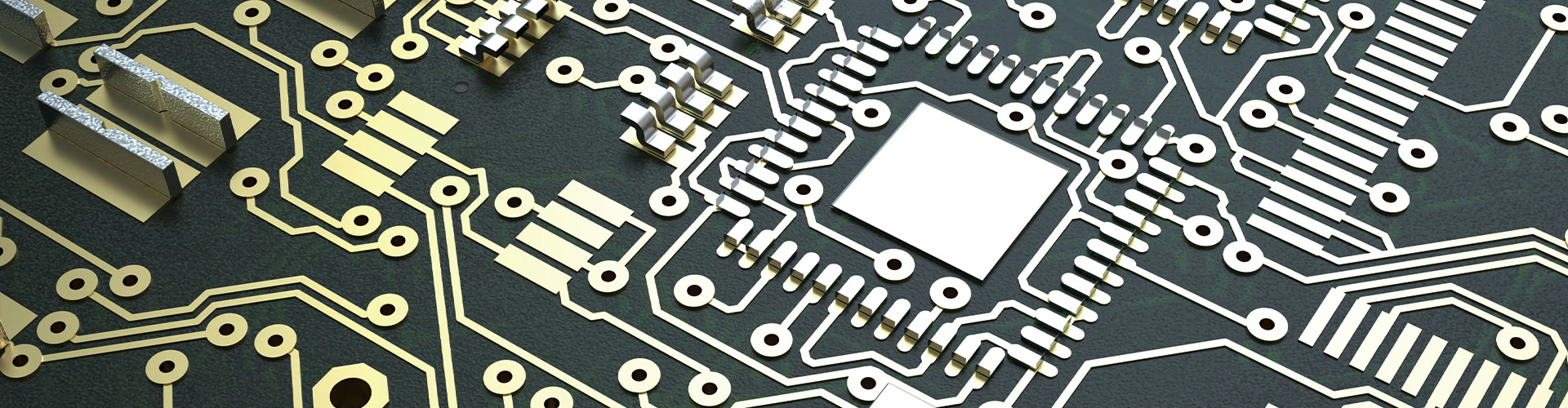
How chiplet and 2.5D/3D packaging shift interconnect onto interposers and substrates, and what that changes for board stack-up, power delivery and release.
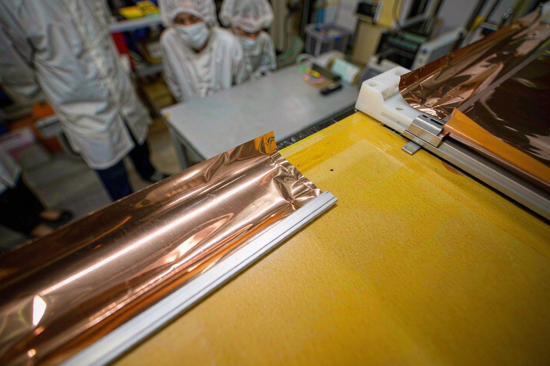
How ultra-thin copper foil down to 12µm improves etch geometry, where it is required for HDI and mSAP builds, and what it costs in handling and yield.