In multi-gigabit digital systems, signal degradation occurs primarily within the dielectric substrate itself rather than through schematic-level logic errors. Successful high speed pcb material selection requires balancing three physical phenomena: dielectric constant ($D_k$), dissipation factor ($D_f$), and the physical weave geometry of the reinforcing fiberglass cloth. If these parameters are incorrectly specified, signals suffer from excessive insertion loss, unpredictable impedance mismatches, and timing skew across differential channels.
This guide provides hardware engineers, layout specialists, and technical procurement teams with an actionable selection framework. It breaks down how dielectric properties shift across operating frequencies, quantifies the impact of resin-to-glass ratios, evaluates woven glass structures, and outlines fabrication steps necessary to preserve signal integrity.
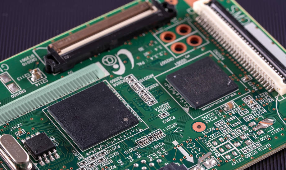
Why Material Selection Dictates Signal Integrity in High-Speed PCBs
Signal integrity is heavily dominated by transmission line physics. As data rates exceed 10 Gbps and enter SerDes architectures operating at 28 Gbps, 56 Gbps (PAM4), and beyond, trace geometries on standard FR-4 cause severe channel attenuation and inter-symbol interference (ISI).
Signal attenuation on a printed circuit board stems from three primary physical loss mechanisms:
Dielectric Loss ($\alpha_d$): Power absorbed by the insulating resin and glass matrix as alternating electric fields polarize molecular dipoles.
Conductor Loss ($\alpha_c$): Resistive dissipation within copper traces, worsened at gigahertz frequencies by the skin effect and surface profile roughness.
Radiation and Coupling Loss: Energy radiated into adjacent structures or leaked via substrate resonant modes.
Standard FR-4 substrates present significant dielectric loss ($D_f \approx 0.015 – 0.020$) and uneven dielectric distribution. At gigahertz frequencies, this causes excessive signal degradation over standard channel reach. Resolving these challenges requires moving to engineered laminates paired with advanced high speed PCB fabrication capabilities to ensure physical layer reliability.
Dielectric Constant ($D_k$): Managing Impedance Stability and Phase Velocity
The real permittivity or dielectric constant ($D_k$, or $\varepsilon_r$) defines the capacitive coupling between a conductor and its reference plane, dictating both characteristic impedance ($Z_0$) and signal phase velocity ($v_p$).
The Physical Impact of $D_k$ on High-Speed Traces
Signal propagation velocity is inversely proportional to the square root of the effective dielectric constant:
$$v_p = \frac{c}{\sqrt{\varepsilon_{\text{eff}}}}$$
Where $c$ represents the speed of light in vacuum and $\varepsilon_{\text{eff}}$ represents the effective relative permittivity. When $D_k$ varies along a transmission path, flight times deviate across parallel traces. In single-ended and differential routing, variations in $D_k$ trigger shifts in line impedance:
$$Z_0 \approx \frac{87}{\sqrt{\varepsilon_r + 1.41}} \ln\left(\frac{5.98h}{0.8w + t}\right)$$
A localized drop or rise in $D_k$ changes the instantaneous trace impedance, introducing signal reflections and degradation at high edge rates. Lower $D_k$ materials permit wider trace widths for a targeted impedance (such as 50 $\Omega$ single-ended or 90/100 $\Omega$ differential), which lowers conductor resistance and reduces overall line attenuation.
Frequency-Dependent $D_k$: Why Nominal Datasheet Values Mislead
Substrate manufacturers often list $D_k$ tested at 1 MHz or 1 GHz using clamped stripline resonator techniques. However, dielectric constant decreases continuously as frequency increases due to dipole relaxation:
Dipole Dispersion: At low frequencies, molecular dipoles track alternating electromagnetic fields. As operational frequencies move into the gigahertz realm, polar molecular groups lag behind the field, lowering measured permittivity.
Effective vs. Bulk $D_k$: In microstrip topologies, electromagnetic fields propagate partially through dielectric substrate and partially through air, producing an effective dielectric constant ($\varepsilon_{\text{eff}}$) lower than the bulk substrate value.
Impact on Stripline Routing: In inner stripline layers, the local resin-to-copper distribution and glass bundle orientation create local deviations from standard vendor-published values.
When calculating stackup dimensions, engineers must extract $D_k$ values measured at the target operational frequency—or the fundamental Nyquist frequency of the intended digital channel—rather than relying on 1 GHz reference metrics.
Dissipation Factor ($D_f$): Minimizing Signal Attenuation at Multi-Gigabit Rates
The dissipation factor ($D_f$, or loss tangent $\tan\delta$) measures the ratio of lost electrical energy to stored electrical energy within a dielectric medium per cycle.
Dielectric Attenuation Dynamics
Dielectric attenuation ($\alpha_d$) increases roughly linearly with frequency:
$$\alpha_d \approx 2.3 \times f \times D_f \times \sqrt{\varepsilon_{\text{eff}}} \quad [\text{dB/inch}]$$
Where $f$ is frequency in gigahertz. As frequency doubles, dielectric absorption doubles. Consequently, while conductor losses dominate at sub-gigahertz frequencies, dielectric loss rapidly overtakes conductor loss in the high-frequency spectrum.
Skin Effect vs. Dielectric Loss: The Crossover Point
At lower operational speeds, current crowds near the conductor surface due to the skin effect, scaling conductor loss proportional to the square root of frequency ($\sqrt{f}$). However, because dielectric loss scales linearly ($f^1$), channels reach a crossover point where substrate choice matters more than trace cross-sectional area:
Below 1 GHz: Conductor resistive loss generally dominates standard laminate channels.
Above 3–5 GHz: Standard FR-4 dielectric losses expand aggressively, often exceeding conductor loss.
At 10 GHz to 28+ GHz: Dielectric loss serves as the primary limiter of channel reach, requiring low-loss or ultra-low-loss resin formulations.
| Material Loss Classification | Typical Df Range (@ 10 GHz) | Typical Dk Range (@ 10 GHz) | Target Interface Rates | Resin System Chemistry |
| Standard Loss (Standard FR-4) | $0.015 – 0.022$ | $4.2 – 4.6$ | $\le 2.5\text{ Gbps}$ ($< 1\text{ GHz}$) | Standard Dicy-cured Epoxy |
| Mid-Loss | $0.010 – 0.014$ | $3.9 – 4.2$ | Up to $5\text{ Gbps} – 8\text{ Gbps}$ | Phenolic-cured modified Epoxy |
| Low-Loss | $0.005 – 0.009$ | $3.6 – 3.9$ | $10\text{ Gbps} – 16\text{ Gbps}$ (PCIe 4.0) | High-Tg Epoxy / PPO / PPE Blends |
| Very Low-Loss | $0.003 – 0.005$ | $3.4 – 3.7$ | $25\text{ Gbps} – 32\text{ Gbps}$ (PCIe 5.0) | Polyphenylene Ether (PPE/PPO) |
| Ultra-Low Loss | $< 0.003$ | $3.0 – 3.5$ | $\ge 56\text{ Gbps} – 112\text{ Gbps}$ (PAM4) | Hydrocarbon / Fluoropolymer / Advanced Thermoset |
The Glass Weave Effect: Unraveling Fiber-Induced Timing Skew
Printed circuit laminates are composed of woven fiberglass cloth impregnated with epoxy or hydrocarbon resin. The fundamental engineering challenge lies in their constituent physical properties:
Standard E-glass Fiber Cloth: $D_k \approx 6.6$
Surrounding Polymer Resin Matrix: $D_k \approx 2.8 – 3.2$
When viewed microscopically, the laminate presents a non-uniform dielectric pattern. Traces routed over this structure cross an alternating surface of dense glass bundles and resin-rich pockets.
| Glass Fabric Architecture | Microscopic Structure & Fiber Distribution | Dielectric Exposure Along Differential Traces | Signal Integrity & Skew Impact | Typical Cloth Styles |
| Standard Open Weave | Loose yarn bundles separated by distinct, unfilled resin windows. | Trace A runs predominantly over glass bundles ($D_k \approx 6.6$); Trace B runs over open resin pockets ($D_k \approx 3.0$). | Severe intra-pair phase skew, rise-time degradation, common-mode noise conversion, and closed eye diagrams. | 106, 1080 |
| Mechanically Spread Glass | Flattened, expanded yarn bundles spread evenly in warp and fill directions. | Both differential legs encounter a continuous, uniform dielectric background ($D_k$ gradients minimized). | Stable propagation delay, minimal intra-pair skew, reduced channel jitter, and preserved eye margins. | 1035, 1067, 1078, 3313 |
Intra-Pair Skew and Differential Degradation
In a high-speed differential channel (e.g., PCIe, USB4, or Ethernet SerDes), one leg of the differential pair may lie over a glass yarn bundle while the complementary leg runs over a resin window.
Because propagation delay depends directly on $\sqrt{D_k}$, the leg over glass experiences higher effective permittivity and travels slower than the leg over resin:
This difference introduces intra-pair skew (propagation time mismatch within the balanced pair).
Skew converts differential-mode signal energy into common-mode noise.
The phase discrepancy closes the receiver eye diagram, degrades jitter tolerance, and induces electromagnetic radiation that can fail regulatory compliance tests.
Mechanical Glass Styles: Open vs. Spread Glass Fabric
Glass fabrics exhibit varied bundle density and window dimensions:
Open Weaves (e.g., Style 106, 1080): Characterized by loose yarn bundles separated by large rectangular resin windows. These styles exhibit significant local $D_k$ variation and should be avoided on critical multi-gigabit routing layers.
Tight Traditional Weaves (e.g., Style 2116, 7628): Denser yarn patterns, but thick glass bundles can complicate micro-via drilling and aspect ratio management.
Spread Glass Fabrics (e.g., Style 1035, 1067, 1078, 3313): Mechanically flattened and spread glass yarns in both warp and fill directions. This manufacturing process closes the resin window, creating an even dielectric background and reducing spatial $D_k$ gradients.
Practical Mitigation Strategies for Designers and Manufacturers
To neutralize the glass weave effect, design and manufacturing teams implement specific mitigation practices:
Specify Spread Glass Laminates: Designate mechanically spread glass fabrics (such as 1067 or 1078) on all layers carrying differential signals operating above 5 Gbps.
Implement Off-Axis or Zig-Zag Routing: Route critical differential traces at an angle (typically $5^\circ$ to $10^\circ$) relative to the orthogonal board edge (x/y weave axis). This ensures both legs of the pair cross equal ratios of glass and resin bundles over distance.
Angle Panelization at Fabrication: If layout constraints prevent angled trace routing on the CAD canvas, work with your manufacturing partner to rotate the entire circuit image $5.5^\circ$ to $10^\circ$ relative to the production master panel.
Dual-Ply Prepreg Usage: Use at least two plies of glass cloth per dielectric core instead of a single thick ply, staggering the yarn bundles to homogenize local permittivity.
Engineering Decision Framework: Matching Substrates to Operating Frequencies
Effective high-speed architecture balances signal margin against bill-of-materials cost. Selecting ultra-low-loss fluoropolymer boards for low-frequency routing inflates production expense without practical benefit. Conversely, under-specifying laminates on high-speed buses causes unrecoverable channel failure.
| Target Data Rate / Frequency | Primary Substrate Classification | Recommended Glass Reinforcement | Conductor Foil Profile | Design & Stackup Recommendations |
| $< 5\text{ Gbps}$ ($< 2.5\text{ GHz}$) | Mid-Loss Substrate ($D_f \le 0.012$, $D_k \approx 4.0$) | Standard dense weave (2116) or Spread (1078) | Standard Electrodeposited (ED) or VLP | Standard orthogonal routing; cost-optimized symmetrical stackup. |
| $5\text{ Gbps} – 16\text{ Gbps}$ ($2.5 – 8\text{ GHz}$) | Low-Loss Substrate ($D_f \le 0.008$, $D_k \approx 3.7$) | Spread Glass Fabric (1067, 1078, 3313) | Very Low Profile (VLP, $R_z < 2\,\mu\text{m}$) | Off-axis/zig-zag routing; dual-ply prepreg configurations; backdrilling stubs $> 0.5\text{ mm}$. |
| $> 16\text{ Gbps} – 56+\text{ Gbps}$ ($> 8 – 28+\text{ GHz}$) | Very Low / Ultra-Low Loss ($D_f \le 0.003$, $D_k \le 3.4$) | Low-$D_k$ Mechanically Spread Glass (1035, 1067, 1078) | Hyper Very Low Profile (HVLP) or Rolled-Annealed Copper | Angle panelization at fab; hybrid stackup architecture; mandatory stub backdrilling $< 0.2\text{ mm}$. |
Application Protocol Matrix
| Interface Protocol | Nyquist Frequency / Baud Rate | Recommended Substrate Loss Class | Glass Style | Copper Foil Requirement |
| PCIe 3.0 / SATA 3.0 | 4 GHz / 8 GT/s | Mid-Loss ($D_f \le 0.012$) | Standard dense weave (2116) or Spread (1078) | Standard Electrodeposited (ED) or Very Low Profile (VLP) |
| PCIe 4.0 / 10GbE | 8 GHz / 16 GT/s | Low-Loss ($D_f \le 0.008$) | Spread Glass (1067, 1078, 3313) | Very Low Profile (VLP) |
| PCIe 5.0 / 25G-SR | 16 GHz / 32 GT/s | Very Low-Loss ($D_f \le 0.004$) | Mechanically Spread Glass mandatory | Hyper Very Low Profile (HVLP) |
| PCIe 6.0 / 56G+ (PAM4) | $\ge 28\text{ GHz} / 56 – 112\text{ Gbps}$ | Ultra-Low Loss ($D_f \le 0.0025$) | Low-$D_k$ Spread Glass fabric | Ultra-smooth HVLP or Rolled-Annealed Copper |
Managing Costs with Hybrid Stackup Architectures
Building high-layer-count boards (16 to 32+ layers) entirely from ultra-low-loss laminates can be cost-prohibitive. To optimize budgets, designers employ hybrid stackups:
High-Speed Routing Layers: Fabricated from low-loss or ultra-low-loss cores (such as advanced modified PPE/PPO or high-frequency thermoset formulations) with spread glass.
Power, Ground, and Low-Speed Signal Layers: Constructed using cost-effective Mid-Loss or high-$T_g$ FR-4 cores.
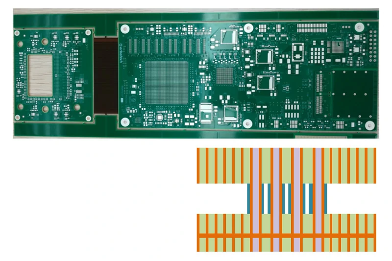
Successful hybrid stackup manufacturing requires close coordination with the fabricator to align coefficient of thermal expansion (CTE), glass transition temperature ($T_g$), and resin cure kinetics across dissimilar materials during panel lamination.
DFM Checklist: Bridging High-Speed Design with Factory Fabrication
Translating simulation parameters into finished circuit boards requires addressing manufacturing practicalities. A stackup calculated in an impedance calculator must withstand factory tolerances, lamination pressure cycles, and wet chemical processes.
When transitioning high-speed designs into production, verify the following design for manufacturability (DFM) requirements:
Pressed Dielectric Thickness Verification: Ensure impedance calculations use the cured, pressed thickness of prepregs rather than nominal raw thicknesses. Resin flows into copper clearance zones during lamination, altering finished dielectric separation.
Copper Roughness Specification: At frequencies above 10 GHz, rough tooth profiles on standard electrodeposited (ED) copper increase conductor loss via signal path elongation. Specify Very Low Profile (VLP) or Hyper Very Low Profile (HVLP) copper foils with treated surface roughness ($R_z$) below $1.5\,\mu\text{m}$.
Impedance Coupon Tolerance Control: Standard PCB tolerances are typically $\pm 10\%$. For high-speed differential traces, evaluate whether your project requires tighter $\pm 5\%$ or $\pm 7\%$ impedance tolerance, verified through serialized Time-Domain Reflectometry (TDR) test coupons.
Backdrilling (Controlled-Depth Counterboring): For signal rates exceeding 10 Gbps, via stubs create resonant quarter-wavelength transmission reflections that form deep notches in channel insertion loss. Specify backdrilling for critical high-speed plated through-holes to reduce remaining stubs below $0.2\text{ mm}$ ($8\text{ mils}$).
Surface Finish Selection: Electroless Nickel Immersion Gold (ENIG) deposits a nickel barrier layer ($D_k$-lossy and ferromagnetic) directly onto the trace surface. High-frequency currents flowing through nickel suffer elevated loss due to the skin effect. For channels exceeding 10–16 Gbps, evaluate Immersion Silver (IAg), Immersion Tin (ISn), or Electroless Nickel Electroless Palladium Immersion Gold (ENEPIG) with thin nickel deposits.
Material Availability and Lead Time: Specialized low-loss laminates frequently carry longer procurement lead times than standard FR-4 variants. Verifying alternative, compatible material callouts on master fabrication drawings prevents project delays.
Through rigorous application of these principles, engineering teams can configure reliable, high-yield boards backed by high speed PCB manufacturing services tailored to complex physical layer constraints.
Key Takeaways
Dielectric Loss Dominates at High Frequency: While conductor losses dictate behavior below 1 GHz, dielectric absorption ($D_f$) and copper surface roughness become the dominant loss mechanisms at 10 GHz and higher.
Frequency-Dependent $D_k$ Governs Impedance: The dielectric constant falls as frequencies climb. Always base layer thickness and trace width geometries on target operational or Nyquist frequencies, not baseline 1 GHz datasheet numbers.
The Glass Weave Effect Generates Timing Jitter: The microscopic permittivity gap between fiberglass bundles ($D_k \approx 6.6$) and resin ($D_k \approx 3.0$) creates intra-pair skew in differential pairs.
Use Established Skew Mitigation Techniques: Flattened spread-glass cloth (e.g., 1067, 1078), angled trace routing, dual-ply prepregs, and off-axis panelization eliminate fiber-induced timing variations.
Optimize Cost via Hybrid Stackups: High-speed systems do not require ultra-low-loss laminates across every layer. Isolating premium substrates to critical high-speed layers lowers overall manufacturing costs.
Account for Fabrication Physical Realities: Factor in pressed dielectric thickness, copper tooth profile (HVLP), backdrilling requirements, and non-magnetic surface finishes during the early stackup simulation phase.
Frequently Asked Questions (FAQ)
Can standard FR-4 be used for signals up to 5 GHz?
Standard FR-4 can function up to 5 GHz only over short channel lengths (typically under 3 to 5 inches) where total insertion loss margins remain loose. However, its high dissipation factor ($D_f \approx 0.018$) rapidly absorbs signal amplitude over longer paths, while open glass weave styles can introduce timing skew. For robust operation at 5 Gbps and above, upgrading to a Mid-Loss or Low-Loss substrate with spread glass cloth provides stable signal margins.
What is the physical difference between E-glass and Low-Dk glass?
Standard E-glass (electrical grade glass) is an aluminoborosilicate formulation with a bulk dielectric constant near 6.6. Low-$D_k$ glass (sometimes designated as NE-glass or L-glass) modifies the oxide composition—reducing heavy metal oxides and altering boron/silica ratios—to lower bulk $D_k$ to between 4.4 and 4.8. This narrower gap between the glass yarn and the surrounding resin matrix significantly reduces local dielectric variations and helps prevent intra-pair skew.
Does surface finish affect high-frequency signal loss?
Yes. Due to the skin effect at multi-gigahertz frequencies, signal currents travel primarily within the outer few microns of the trace, passing through the surface finish plating. Standard ENIG features a nickel barrier layer that is ferromagnetic and presents higher electrical resistance than copper, increasing insertion loss at frequencies above 10 GHz. Finishes such as Immersion Silver (IAg), Immersion Tin (ISn), or surface-preserving organic solders provide a cleaner conductive interface with lower insertion loss.
How does copper foil roughness interact with $D_f$ at high frequencies?
While $D_f$ measures dielectric absorption, surface roughness directly magnifies conductor loss. As the skin depth drops below $1\,\mu\text{m}$ at multi-gigahertz frequencies, current must follow the microscopic contours of the copper tooth profile, effectively increasing path resistance. Furthermore, rough tooth profiles alter the local electric field distribution, raising the apparent capacitance and effective $D_k$. Using VLP or HVLP copper foils ensures that low-$D_f$ laminates achieve their simulated attenuation metrics.