Effective high-speed PCB stackup design requires balancing three conflicting engineering variables: maintaining signal integrity through tightly controlled impedance paths, managing parasitic coupling and loop inductance, and minimizing manufacturing layer count to contain fabrication costs. A successful stackup defines trace geometries and reference plane arrangements so signals propagate without timing jitter, reflections, or radiated emissions, while remaining feasible for standard factory lamination presses.
Achieving this balance depends on choosing laminate materials with suitable dielectric properties (Dk and Df), arranging continuous solid reference planes for uninterrupted return paths, and accommodating routing density without adding unnecessary layers. This guide breaks down the physical rules governing layer distribution, compares substrate material loss performance, evaluates stackup architectures from 4 to 12 layers, and outlines standard procedures for aligning impedance simulations with production line tolerances.

The Engineering Dilemma: Signal Integrity vs. Layer Count vs. Fabrication Cost
In high-speed digital systems, stackup definition acts as the primary hardware constraint for electromagnetic compatibility (EMC) and signal transmission quality. Low-speed designs often permit arbitrary layer assignments and split planes. In contrast, modern high-speed designs operating with fast edge rates (sub-nanosecond rise and fall times) treat every copper trace as an electromagnetic waveguide.
| Engineering Dimension | Primary Technical Objective | Risk When Compromised | Impact on Other Variables |
| Signal Integrity (SI & EMC) | Preserve edge rates, contain crosstalk, and ensure continuous return current loops without emissions. | Severe reflections, timing jitter, ground bounce, and EMC laboratory test failures. | Requires dedicated reference planes and controlled dielectric heights, often demanding higher layer counts. |
| Layer Count & Density | Accommodate fine-pitch BGAs, escape routing, and isolation channels within a manageable board thickness. | Congested routing channels, unintended broadside coupling, and routing across plane splits. | Compressing layer counts degrades return path continuity; expanding layer counts escalates fabrication expense. |
| Manufacturing Cost & Yield | Maintain standard lamination cycles, viable drilling aspect ratios, and reliable layer-to-layer registration. | Scrap from press misregistration, plating voids in high aspect-ratio vias, and high unit board costs. | Aggressive cost reduction (fewer layers, generic FR-4) directly degrades controlled impedance and signal fidelity. |
When engineers encounter crosstalk or high routing density, the intuitive reaction is to add board layers. However, every additional layer pair introduces measurable trade-offs:
Direct Cost Escalation: Core laminates, prepreg sheets, and additional pressing cycles increase bare-board fabrication costs linearly or exponentially, especially if blind or buried microvias are introduced.
Aspect Ratio and Registration Risks: Higher overall thickness increases the via aspect ratio (board thickness to drill hole diameter), complicating copper plating inside through-holes and raising registration error rates across press lamination cycles.
Performance Penalties of Under-Layering: Conversely, prematurely compressing an 8-layer architecture into a 4-layer or 6-layer board forces high-speed differential traces over split power domains or adjacent to unshielded signal layers, creating severe impedance discontinuities, ground bounce, and radiated emissions that often fail EMC laboratory testing.
A successful stackup manages these trade-offs early in the design cycle, before trace routing begins.
Core Electrical Principles: Ground Reference, Return Paths, and Crosstalk
A high-speed signal does not travel strictly through the copper trace; the electromagnetic energy propagates through the dielectric between the trace and its immediate reference plane. The return current always follows the path of least impedance (dominated by lowest loop inductance at high frequencies), directly underneath the signal conductor.
Unbroken Reference Planes and Return Current Loops
| Reference Configuration | Physical Plane Structure | Return Current Path Behavior | Signal Integrity & EMC Result |
| Continuous Reference Plane (Best Practice) | Unbroken solid copper sheet directly underneath the signal trace. | Mirrors trace directly beneath conductor along the path of least loop inductance. | Controlled characteristic impedance, minimal loop area, low radiation, and preserved eye margins. |
| Split Plane Discontinuity (Design Hazard) | Signal trace crosses an isolation slot, power cut, or split ground domain. | Diverts around slot perimeter to find nearest ground via or DC stitching capacitor. | Loop area expands into an unintended antenna, elevating loop inductance, reflections, and EMI. |
Avoid Plane Splits: A reference plane underneath a high-speed microstrip or stripline must remain unbroken. Routing across a split or slot forces return current to take a wide detour around the void, raising inductance and generating significant reflections.
Microstrip vs. Stripline Placement:
Microstrip (Outer Layers): Offers faster propagation velocity due to lower effective dielectric constant (a hybrid of laminate Dk and air), but radiates energy directly into the environment and remains susceptible to external noise.
Stripline (Inner Layers): Sandwiched between two solid ground planes, stripline geometry provides superior electromagnetic shielding and reduced crosstalk, making it the preferred routing strategy for sensitive high-speed lines, despite slightly higher dielectric losses.
Power-Ground Plane Coupling and Interplane Capacitance
Placing a power plane immediately adjacent to a solid ground plane with a thin dielectric core creates high-frequency interplane capacitance. This structural capacitance provides low-inductance power delivery that dampens power-rail ripple at frequencies where discrete surface-mount decoupling capacitors lose effectiveness due to mounting parasitic inductance.
Selecting Substrate Materials: Balancing Dk, Df, and Thermal Stability
The dielectric material defines signal attenuation, propagation delay, and phase stability across operating frequencies. Substrate selection requires balancing loss budgets with raw material expense.
When Standard FR-4 Fails: Frequency Thresholds and Loss Budgets
Standard FR-4 is cost-effective for general electronics, but its loss characteristics degrade signal quality as edge rates sharpen and clock frequencies climb:
Dielectric Constant ($D_k$): Standard FR-4 exhibits a $D_k$ around 4.2 to 4.5. This value shifts noticeably across frequency bands, causing dispersion where different frequency components of a digital signal travel at different velocities, degrading the signal eye opening.
Dissipation Factor ($D_f$ / Loss Tangent): FR-4 has a typical $D_f$ between 0.015 and 0.020. At frequencies above a few gigahertz, dielectric loss overtakes copper resistive loss as the primary source of signal attenuation.
For high-speed interfaces like PCIe 4.0/5.0, 10G+ Ethernet, or high-data-rate DDR buses, high-speed laminates with tightly controlled resin contents and low loss tangents are required to preserve signal integrity over transmission distances.
| Material Category | Typical Dielectric Constant (Dk) | Typical Loss Tangent (Df) | Relative Material Cost | Common Application Profile |
| Standard FR-4 | 4.2 – 4.5 | 0.015 – 0.020 | Baseline (1.0x) | Low-speed microcontrollers, simple boards, signals $< 1 \text{ GHz}$ |
| Mid-Loss Laminate | 3.9 – 4.1 | 0.010 – 0.012 | 1.3x – 1.8x | DDR4, PCIe 3.0, gigabit transceivers, mid-length traces |
| Low-Loss Laminate | 3.5 – 3.8 | 0.004 – 0.008 | 2.0x – 3.0x | PCIe 4.0/5.0, 25G NRZ interfaces, high-density backplanes |
| Ultra-Low-Loss (PTFE/Hydrocarbon) | 3.0 – 3.5 | 0.001 – 0.003 | 4.0x – 8.0x+ | RF/Microwave radar, 56G/112G PAM4 optical systems |
Note: Specific laminate families, copper roughness profiles (such as Very Low Profile or HVLP foil), and exact resin recipes should be evaluated against raw board costs by coordinating with a custom high-speed PCB fabrication specialist to verify supplier inventories and lead times.
Layer Count Optimization: 4-Layer, 6-Layer, and 8-Layer+ Architectures
Selecting the correct layer count requires evaluating channel counts, package pinout densities (such as fine-pitch BGAs), and electrical isolation demands.
| Layer Stackup Type | Layer Assignment Mapping | Primary Electrical Advantages | Key Engineering Limitations |
| 4-Layer (Optimized) | L1: Signal / Fast Traces
L2: Solid GND
L3: Solid GND or Power
L4: Signal / Non-Critical |
Excellent reference coupling for outer traces; minimal layer count and lowest manufacturing cost. | Limited routing channels; power distribution often requires copper pours on outer layers or split planes on L3. |
| 6-Layer (Balanced Stripline) | L1: Component / High-Speed Microstrip
L2: Solid GND
L3: High-Speed Stripline
L4: Dedicated Power Plane
L5: Solid GND
L6: Component / Low-Speed Signals |
Clean stripline shielding on L3 referenced to solid ground; interplane capacitance between L4 and L5. | L1 and L6 remain exposed to radiation; routing density remains tight for multi-channel BGA escape. |
| 8-Layer (Dual-Stripline) | L1: Outer Microstrip
L2: Solid GND
L3: High-Speed Stripline 1
L4: Solid GND
L5: Core / Power Plane
L6: High-Speed Stripline 2
L7: Solid GND
L8: Outer Microstrip |
Dual embedded stripline channels (L3 & L6) completely isolated by dedicated ground planes; zero broadside crosstalk. | Increased raw material and lamination cost; requires strict dielectric symmetry to prevent board warpage. |
4-Layer and 6-Layer Stackups: Limitations and Mitigation Strategies
4-Layer Architecture:
Traditional Structure (SIG – GND – PWR – SIG): Placing outer signal layers over inner planes separates traces from returns by a core thickness, which is often 30 to 40 mils thick. This large distance causes wide trace geometries for 50-ohm targets and poor high-frequency coupling.
Optimized Structure (SIG – GND – GND/PWR – SIG): Utilizing thin prepreg outer dielectrics (e.g., 3 to 5 mils) places signal lines directly over a continuous ground plane on Layer 2, delivering tight impedance control and small return loops.
6-Layer Architecture:
The 6-Layer Trade-off: Standard 6-layer construction (SIG – GND – SIG – PWR – GND – SIG) often leaves the middle signal layer (L3) referenced ambiguously between a ground plane and a split power plane, risking unexpected return path discontinuities.
Recommended Configuration: Group critical high-speed routing on Layer 3 referenced against a solid ground plane on Layer 2, dedicate Layer 4 to low-noise power planes, and place a second ground plane on Layer 5. This provides clean stripline propagation on Layer 3 while isolating high-speed signals from power transients.
8-Layer to 12-Layer Stackups: The Sweet Spot for High-Density Signal Integrity
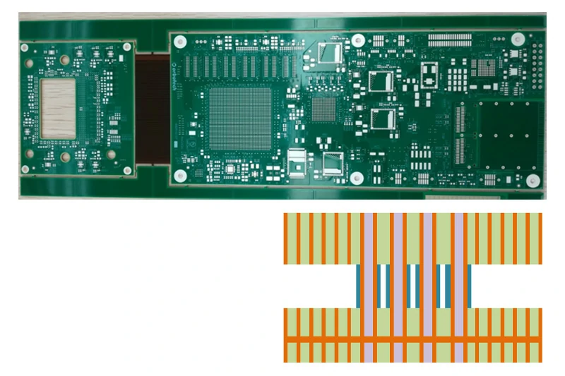
For dense BGA layouts and high-speed multi-lane buses, 8-layer and 10-layer configurations provide symmetric, isolated routing corridors:
The 8-Layer Dual-Stripline Model: (SIG1 – GND1 – SIG2 – GND2 – PWR – SIG3 – GND3 – SIG4). This setup provides continuous ground references for both inner stripline layers (L3 and L6) and eliminates broadside crosstalk by interposing solid reference planes between adjacent signal channels.
Preserving Symmetry: Stackup layups must remain mechanically symmetric across the center core (matching dielectric thicknesses, prepreg types, and copper foil weights) to prevent thermal stress imbalances that lead to board twisting and warpage during reflow soldering.
Reviewing stackup options against confirmed high-speed PCB manufacturing capabilities ensures that specified core/prepreg ratios comply with standard pressing clearances and inner-layer registration tolerances.
Practical Controlled Impedance: Bridging Field Solvers and Factory Floors
Designing an accurate stackup requires bridging the gap between theoretical EDA 2D field solvers and real-world PCB factory processes.
| Stage | Cross-Sectional Geometry | Dimensional Representation | Source of Variation / Discrepancy |
| EDA Field Solver Model | Idealized Rectangle | Nominal Width ($W$), Uniform Thickness ($T$) | Assumes vertical sidewalls, uniform dielectric constant, and perfectly flat copper foil. |
| Fabricated Board (Factory Floor) | Trapezoid | $W_{\text{top}} \approx W – \Delta W$, $W_{\text{bottom}} \approx W$ | Chemical etching cuts laterally under resist masks (etch factor), narrowing the trace top. |
| Pressed Prepreg Matrix | Resin-Wetted Fibers | Compressed Thickness ($H_{\text{pressed}} < H_{\text{nominal}}$) | Liquid resin redistributes into copper void patterns under heat and pressure, shifting final height. |
Single-Ended (50Ω) and Differential (90Ω/100Ω) Target Rules
High-speed protocols operate under standardized characteristic impedance targets:
Single-Ended Signaling: Typically targeted at $50\Omega \pm 10\%$ (often used in control lines, DDR data channels, and single-ended clock paths).
Differential Signaling: Targeted at $100\Omega \pm 10\%$ (Ethernet, PCIe, SATA) or $90\Omega \pm 10\%$ (USB 2.0 / USB 3.x).
Trace-to-Space Geometry: Achieving a differential target requires balancing trace width ($W$) and differential spacing ($S$) against dielectric height ($H$) to the reference plane. Moving a trace closer to its ground plane lowers impedance, requiring a narrower copper trace to restore the 50-ohm baseline.
Factory Process Variations: Etch Factor, Prepreg Flow, and Dielectric Tolerances
A common source of board redesigns is failing to account for physical etching and pressing variations:
The Etch Factor (Trapezoidal Cross-Sections): Chemical etching removes copper from the sides as well as the top, turning an ideal rectangular trace cross-section into a trapezoid. If this top-versus-bottom width variance is omitted from impedance calculations, final trace impedance will measure higher than simulated.
Resin Flow and Glass Weave Inhomogeneity: During hot lamination, resin flows to fill copper voids, reducing the final pressed dielectric thickness compared to uncured sheets. Furthermore, differential traces routed parallel to loose glass weaves can cause phase skew, where one trace of a differential pair sits over glass bundles while the companion trace sits over resin pockets. Specifying spread-glass fabrics (e.g., 1078 or 3313 styles) mitigates weave-induced timing jitter.
Impedance Coupon Verification: Factory production panels include edge test coupons that mirror the design’s trace-to-plane configurations. Using Time-Domain Reflectometry (TDR), the manufacturer measures signal reflections and verifies that real-world trace batches land within target impedance windows prior to board routing and shipping.
Engineering teams should source panels through verified controlled impedance PCB fabrication workflows to lock down resin recession tolerances and confirm copper etch allowances before freezing artwork.
Pre-Layout Stackup Verification Checklist
Use this checklist to verify engineering and manufacturing parameters before committing to component layout and routing:
Continuous Ground References: Are all critical high-speed routing layers positioned immediately adjacent to a solid, unbroken ground reference plane?
Mechanical Layer Symmetry: Is the stackup balanced symmetrically across the center axis in copper weight, dielectric core thicknesses, and prepreg styles to prevent board warpage?
Material Loss Compatibility: Has the substrate material loss tangent ($D_f$) been validated against the system channel loss budget at the maximum Nyquist frequency?
Minimum Core & Prepreg Limits: Are the chosen dielectric layers thick enough to prevent dielectric breakdown while remaining compatible with standard fabricator prepreg flows?
Trace Width Manufacturability: Are the calculated trace widths and differential line spaces compatible with standard manufacturing etching limits (typically $\ge 3.5 / 3.5\text{ mils}$ for standard-yield processing)?
Aspect Ratio Verification: Does the total board thickness versus smallest drilled via hole stay within standard mechanical drilling ratios (typically $\le 10:1$ for through-hole vias)?
Glass Weave Style: Are high-data-rate differential channels ($>10\text{ Gbps}$) specified with spread-glass fabrics to avoid weave-induced timing skew?
Power-Ground Plane Pairing: Are main DC power planes positioned closely adjacent to continuous ground planes to maximize interplane decoupling capacitance?
Streamlining Your Stackup: Engage Your Manufacturer Early
Achieving signal integrity, predictable impedance, and optimal layer counts requires continuous trade-offs between theoretical transmission line physics and manufacturing limits. Attempting to finalize trace widths and differential pairs in isolation often leads to impedance shifts, re-spins, and unnecessary cost increases when production begins.
Involving an experienced high-speed PCB manufacturer before freezing board dimensions and layout constraints ensures that standard lamination materials, copper thicknesses, and tooling profiles are used from the start. This early collaboration confirms core resin selections, validates glass styles, and matches 2D field solver outputs directly to factory floor tolerances.
Key Takeaways
Stackup Dictates Signal Integrity: In high-speed board design, trace impedance, signal attenuation, and electromagnetic radiation are fundamentally determined by layer placement, plane continuity, and dielectric properties rather than routing topology alone.
Ground Planes Are Primary Return Conduits: Return current naturally follows the path of least inductance directly under high-speed traces. Routing across split reference planes induces significant reflections, ground bounce, and EMI compliance failures.
Choose Laminates by Loss Budgets: While standard FR-4 works for sub-gigahertz routing, designs utilizing high-speed serial links (such as PCIe 4.0/5.0 or high-rate DDR) require mid-loss or low-loss laminates with low dissipation factors ($D_f$) and spread-glass weaves to prevent channel loss and phase skew.
Symmetry Prevents Warpage: Stackups must maintain mechanical balance in dielectric thickness and copper distribution above and below the center core to prevent thermal stress warpage during automated assembly.
Close the Simulation-to-Factory Gap: Nominal trace models must account for real-world manufacturing variations—including trapezoidal etch factors and resin flow-down—using TDR coupon testing to guarantee final impedance targets.
Frequently Asked Questions (FAQ)
How do I determine if a design requires low-loss laminates instead of standard FR-4?
The choice depends on your operating frequency, signal rise times, and total trace length. When channel insertion loss calculations at the target Nyquist frequency exceed system receiver thresholds—typically seen in links running beyond 5 to 8 Gbps over traces longer than a few inches—the dissipation factor ($D_f$) of standard FR-4 introduces unacceptable eye closure, requiring an upgrade to mid-loss or low-loss materials.
Can a 4-layer PCB support high-speed differential interfaces like USB 3.0 or DDR memory?
A 4-layer stackup can support modest-length high-speed lines only if configured with thin outer prepregs over continuous inner ground/power planes (e.g., Signal – Ground – Ground/Power – Signal). However, routing dense interfaces like DDR with matched lengths and tight timing margins is difficult on 4 layers due to limited routing channels and the risk of breaking reference planes around dense via fields.
What is the standard impedance tolerance for high-speed controlled impedance PCBs?
The industry-standard tolerance for controlled impedance traces is $\pm 10\%$. Tighter tolerances of $\pm 7\%$ or $\pm 5\%$ can be achieved under specific manufacturing conditions, but they require tighter raw material controls, specialized etch compensation, and frequent coupon verification, which can impact overall fabrication yields and costs.
Why do high-speed stackups require mechanical balance and symmetry?
PCB stackups must be balanced across their horizontal center axis in terms of core thickness, prepreg volume, and copper foil distribution. An asymmetric build creates uneven thermal expansion stresses during high-temperature reflow soldering, resulting in board twisting, bow, and warpage that compromises solder joint integrity on fine-pitch components.