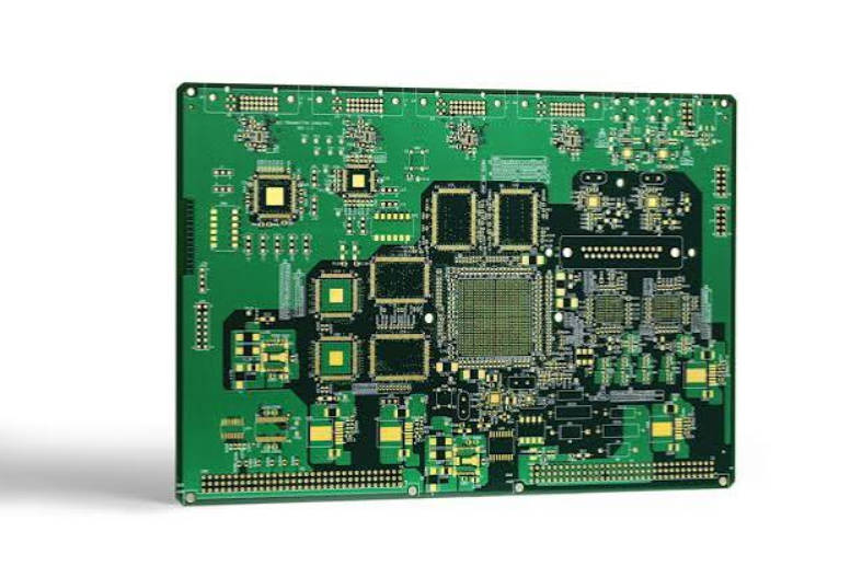
In digital and RF hardware development, a circuit transitions into a high-speed design not because of its clock frequency, but because of its signal rise and fall times. When signal transition times become shorter than the round-trip propagation delay across a copper trace, standard layout rules cease to function, and distributed transmission line behavior takes over.
Precise mastery of high-speed PCB terminology bridges the critical gap between conceptual signal integrity simulation and bare-board fabrication. Misinterpreting terms like insertion loss, phase skew, anti-pad clearance, or weave alignment can quickly lead to failed eye diagrams, unresolvable electromagnetic interference (EMI), and costly scrap runs.
This technical guide categorizes 45 essential terms across signal integrity, routing geometry, substrate properties, and fabrication verification, helping engineering teams specify boards accurately and navigate high-speed PCB fabrication with clear design-for-manufacturing (DFM) alignment.

Signal Integrity Fundamentals: Core Terms Governing High-Frequency Signals
Signal integrity fundamentals describe how an electrical waveform behaves once edge rates shrink below the propagation delay of the interconnect.
Signal integrity (SI) focuses on preserving electrical waveform quality as energy travels from driver pins across the printed circuit board to receiver ICs.
1. Rise Time (tr)
The time required for an electrical signal edge to transition between two specified voltage levels—typically from 10% to 90% (or 20% to 80%) of its final amplitude. Rise time, rather than repetitive clock rate, defines the maximum frequency content (fmax ≈ 0.35 / tr) present on the interconnect.
2. Propagation Delay (tpd)
The duration required for an electromagnetic wave to travel across a unit length of a PCB trace, expressed in picoseconds per inch (ps/in) or picoseconds per millimeter (ps/mm). Propagation delay depends directly on the effective dielectric constant (εr,eff) of the surrounding laminate.
3. Critical Length (Lcrit)
The physical trace length threshold beyond which transmission line effects must be evaluated to prevent reflections. A common rule of thumb defines critical length as:
Traces exceeding this length require termination networks and controlled characteristic impedance.
4. Characteristic Impedance (Z0)
The ratio of high-frequency voltage to current propagating down an infinitely long, uniform transmission line. It is determined solely by the trace cross-sectional geometry, dielectric spacing, and substrate permittivity—not by the physical length of the trace. See controlled impedance for how this is held on the fabricated board.
5. Reflection Coefficient (Γ)
A quantitative measure of how much signal energy reflects back toward the source when a propagating wave encounters an impedance discontinuity. It is calculated as:
Where ZL represents load impedance and Z0 represents transmission line characteristic impedance.
6. Return Loss (S11)
The ratio of reflected power to incident power at a channel port, expressed in decibels (dB). Lower negative values (or higher absolute dB figures in positive notation) indicate better impedance matching and minimal signal reflection along the interconnect.
7. Insertion Loss (S21)
The total attenuation of signal power as it travels through a channel from input to output, expressed in dB. Insertion loss aggregates conductor dielectric losses, copper surface roughness attenuation, and radiation dissipation across operational frequencies.
8. Near-End Crosstalk (NEXT)
Unintended electromagnetic coupling detected on a quiet transmission line at the end nearest the active driver of an adjacent aggressor line. NEXT energy begins immediately when the aggressor switches and flows directly back toward the receiver on the victim line.
9. Far-End Crosstalk (FEXT)
Coupling observed on an adjacent quiet line at the destination receiver furthest from the aggressor’s driving source. FEXT depends on asymmetries in capacitive and inductive mutual coupling coefficients, which often cancel out in uniform homogeneous stripline geometries but remain active in microstrip routing.
10. Jitter
The short-term, unwanted temporal displacement of a digital signal’s significant edges from their ideal, theoretical clock positions. Jitter is categorized into deterministic jitter (bounded mechanisms like crosstalk and duty-cycle distortion) and random jitter (unbounded Gaussian thermal noise).
11. Skew
The differential delay or time offset between two physical signals. Intrapair skew defines the arrival-time difference between the true and complement traces of a differential pair, while interpair skew denotes the latency difference between distinct parallel clock and data lanes.
12. Eye Diagram
An oscilloscope or simulation display created by repetitively overlaying data transitions across multiple unit intervals (UI). Key metrics derived from the eye diagram include eye height (representing noise margin), eye width (representing timing jitter margin), and jitter at cross-points.
Geometry & Stackup Terminology: Routing and Waveguide Structures
How copper traces are configured against adjacent dielectric cores, prepregs, and reference planes determines both trace impedance stability and susceptibility to noise.
| Routing Structure | Layer Position | Reference Plane Configuration | Surrounding Dielectric Medium | Typical Application |
|---|---|---|---|---|
| Microstrip | Outer Layer (Top / Bottom) | Single reference plane directly underneath | Asymmetric / Inhomogeneous (Laminate below, Solder Mask + Air above) | High-speed component fanout, short interconnects |
| Stripline | Inner Layer | Two reference planes (Symmetrical or Asymmetrical) | Homogeneous (Fully encapsulated in Core / Prepreg dielectric) | Long-reach multi-gigabit differential pairs, EMI-critical buses |
| Grounded Coplanar Waveguide (GCPW) | Outer or Inner Layer | Underlying plane + Coplanar ground traces flanking both sides | Mixed dielectric with lateral ground fences | RF, microwave, and millimeter-wave trace isolation |
13. Differential Impedance (Zdiff)
The total impedance measured between a pair of complementary, coupled signal traces driven with equal-magnitude, opposite-polarity signals. It is expressed roughly as Zdiff ≈ 2 × Z0 × (1 − k), where k represents the mutual electromagnetic coupling factor between the two lines.
14. Odd-Mode Impedance (Zodd)
The impedance of a single trace within a differential pair when both lines are driven with differential (equal and opposite) signals. Under balanced conditions, Zdiff = 2 × Zodd.
15. Even-Mode Impedance (Zeven)
The impedance of a single trace in a pair when both conductors are driven simultaneously with identical (common-mode) signals of the same polarity and amplitude.
16. Microstrip
A transmission line routed on an outer layer of a PCB, separated from a single underlying reference plane by a dielectric layer. Because air (εr ≈ 1.0) and solder mask sit on top while core/prepreg sits below, microstrip lines propagate signals in an inhomogeneous medium, causing higher radiation and distinct forward crosstalk.
17. Stripline
A transmission line embedded entirely within internal PCB layers, positioned symmetrically or asymmetrically between two continuous reference planes. Stripline provides excellent EMI shielding and uniform dielectric properties, which eliminates far-end crosstalk under ideal routing conditions.
18. Coplanar Waveguide (CPW)
A transmission line configuration where ground conductors are routed on the same layer on both sides of the center signal trace, separated by a specified gap. When backed by a solid reference plane beneath the dielectric, it is known as Grounded Coplanar Waveguide (GCPW), widely used in RF and millimeter-wave boards for isolation.
19. Return Path
The continuous loop through which high-frequency return currents traverse reference planes back to the signal source. At high frequencies, return current does not follow the path of least electrical resistance; it follows the path of minimum loop inductance, concentrating directly underneath or above the signal trace.
20. Split Plane Crossing
A design hazard that occurs when a high-speed trace routes directly over a gap, void, or split between distinct ground or power planes. Crossing a plane split breaks the path of least inductance, forcing return currents to divert around the opening, creating substantial loop inductance, signal degradation, and EMI radiation.
21. Ground Bounce (Simultaneous Switching Noise – SSN)
A transient voltage shift across reference ground networks caused by rapid current variations (di/dt) through stray parasitic inductances (L) of component pins, wire bonds, and vias, governed by:
22. Length Matching (Delay Tuning)
The practice of equalizing the physical length—and consequently the propagation flight time—of critical traces across differential pairs or parallel buses. Tolerances are covered in length matching and delay tuning rules.
23. Meander / Trombone Routing
Specific geometric routing patterns (accordion or serpentine folds) inserted along shorter traces to equalize path delay with adjacent longer traces. The spacing between adjacent folds must remain sufficiently wide (typically > 3× to 4× trace width) to prevent unwanted self-coupling and signal dispersion.
24. Reference Plane
An unbroken copper layer (either ground or a well-decoupled DC power plane) running parallel to a signal trace layer to provide a constant return path and establish consistent characteristic impedance.
| Trace Topology | Reference Planes | Typical Propagation Velocity | EMI Shielding | Fab Complexity |
|---|---|---|---|---|
| Microstrip | 1 (Underneath) | Faster (≈ 150–170 ps/in) | Low (Trace exposed) | Standard outer-layer etches |
| Stripline | 2 (Top and Bottom) | Slower (≈ 170–190 ps/in) | High (Fully shielded) | Precise prepreg thickness control |
| Grounded CPW | 1 Underlying + Co-planar Ground | Intermediate | High (Adjacent copper walls) | Requires tight trace-to-copper gap etching |
Substrate Materials & Dielectric Properties
Substrate selection governs signal loss, thermal survival, and timing consistency across multi-gigahertz channels.
25. Dielectric Constant (Dk / εr)
The relative permittivity of a material, representing its ability to store electrostatic energy relative to a vacuum. Lower dielectric constant values yield faster signal propagation velocities and allow wider trace widths for a given target impedance, reducing resistive copper loss.
26. Dissipation Factor (Df / tanδ)
The ratio of energy dissipated into heat versus energy stored in the dielectric per cycle, also known as loss tangent. Low-Df laminates are critical for multi-gigabit serial channels (such as PCIe 5.0/6.0 and 112G PAM4) to minimize total dielectric attenuation.
27. Glass Weave Effect
Timing skew and impedance fluctuations that occur when differential traces route unevenly over the alternating fiberglass bundles and resin pockets of a woven PCB core. Because the dielectric constant of glass (≈ 5.5–6.5) differs notably from typical epoxy resin (≈ 3.0–3.5), a trace sitting over a glass bundle exhibits a different propagation speed than its pair sitting over resin. See glass weave effect and fiber weave skew.
28. Mechanically Spread Glass
Substrate fabric constructed with flattened, uniformly spread fiberglass yarns. By minimizing gaps between fiber bundles, spread glass produces a homogeneous dielectric profile across the panel, mitigating intrapair skew without requiring aggressive angled routing.
29. Skin Depth (δ)
The depth into a conductor at which high-frequency alternating current density falls to 1/e (roughly 37%) of its surface value:
As signal frequencies rise into gigahertz regimes, current concentrates almost entirely in a microscopic outer ring of the copper trace.
30. Skin Effect
The phenomenon where high-frequency current concentrates along the outer perimeter of a conductor rather than spreading uniformly across its cross section. This dramatically increases the effective AC resistance and ohmic attenuation of the interconnect.
31. Copper Surface Roughness (Profile)
The micro-topography of copper foil bonded to PCB prepreg cores. While mechanical tooth profiles are necessary for laminate adhesion, high surface peaks force high-frequency current travelling within the shallow skin depth to traverse a longer, tortuous path, significantly increasing conductor insertion loss.
| Copper Foil Grade | Profile Depth (Rz / Sq) | Skin Effect & Current Path Dynamics | High-Frequency Insertion Loss Impact | Suitable Speed / Frequency Regimes |
|---|---|---|---|---|
| Standard Electrodeposited (STD ED) | High (Rz ≥ 5–10 μm) | Current follows tortuous peaks and valleys; effective path length increases significantly | Severe attenuation at gigahertz frequencies | Standard low-speed digital; DC power; < 1 GHz |
| Very Low Profile (VLP) | Moderate (Rz ≈ 2–3 μm) | Moderately flattened tooth structure; current path distortion reduced | Moderate attenuation; balanced adhesion and loss | 5–16 Gbps (e.g., PCIe 3.0 / PCIe 4.0) |
| Hyper Very Low Profile (HVLP) / Profile Free | Minimal (Rz ≤ 1.5 μm) | Smooth boundary surface; current travels along a direct, linear electrical path | Lowest conductor loss; preserves channel margin | ≥ 25–112 Gbps (e.g., PCIe 5.0/6.0, 112G PAM4) |
32. Glass Transition Temperature (Tg)
The temperature boundary at which an amorphous cured resin transitions from a rigid, glassy state into a softer, rubbery state. High-speed, high-density interconnect (HDI) boards generally require Tg ≥ 170℃ to withstand lead-free reflow heat without delaminating.
33. Decomposition Temperature (Td)
The thermal point at which a PCB material permanently loses 5% of its original mass through chemical breakdown. Td must safely exceed assembly soldering profiles to prevent inner-layer degradation.
34. Coefficient of Thermal Expansion (CTE)
The fractional rate at which a substrate expands per degree of temperature change, measured along the X, Y, and Z axes. Controlling Z-axis CTE (ppm/℃) is especially vital for preventing barrel cracking in plated through-holes (PTH) during repeated thermal shocks.
PCB Fabrication, Interconnect & Testing Terminology
A simulation remains purely theoretical until translated into physical tolerances on the manufacturing floor.
35. Via Stub
The unused electrical portion of a plated through-hole via barrel extending beyond the connected internal layer. A via stub acts as an unterminated, open-ended transmission line stub. At its quarter-wavelength resonant frequency, the stub draws energy out of the signal path, creating severe notches in the insertion loss spectrum.
36. Backdrilling (Controlled-Depth Counterboring)
A secondary drilling operation that uses a drill bit slightly larger than the original hole diameter to remove unused via stubs from the reverse side of the panel, eliminating stub resonance in high-speed channels. Drill tolerances are covered in via design and DFM checks.
| Via Configuration | Mechanical Structure | Electrical Behavior | High-Speed Performance Impact | Primary DFM Consideration |
|---|---|---|---|---|
| Standard Plated Through-Hole (PTH) | Full-barrel copper cylinder penetrating all layers | Signal exits at inner layer; remaining barrel forms an open stub | Stub creates resonant frequency notches and signal reflections | Standard drilling process; no secondary drill passes |
| Backdrilled Through-Hole | PTH with unused barrel section mechanically drilled out from reverse side | Signal path preserved; remaining stub length minimized (typically ≤ 0.2 mm) | Eliminates stub resonance; restores high-frequency channel bandwidth | Requires controlled-depth drill tolerance (± 0.05 mm) and dedicated layer pair callouts |
| Laser Microvia (HDI) | Blind, shallow-depth cone spanning a single dielectric layer | Direct layer-to-layer connection without extending into unrouted layers | Zero stub parasitics; minimal capacitance and inductance | Limited layer span (≤ 150 μm depth); requires microvia stack/stagger design rules |
37. Blind Via
A plated hole that originates on an external surface layer and terminates at an internal layer, without traversing through the remaining thickness of the board.
38. Buried Via
A plated hole contained entirely within internal cores of the PCB, with no opening or physical contact with the external surface layers.
39. Microvia
A small-diameter via—typically ≤ 150 μm (0.006 in)—drilled using a laser and spanning a single dielectric layer. Microvias introduce negligible parasitic capacitance and inductance compared to mechanical through-holes, making them the primary building block for high-speed HDI stackups.
40. Anti-Pad (Plane Clearance)
The clearance cutout etched into a copper power or ground plane where a via passes through without electrical contact. Sizing the anti-pad correctly balances reference plane return continuity against parasitic capacitive loading between the via barrel and the adjacent copper.
41. Time-Domain Reflectometry (TDR)
A test method that injects a fast-rising voltage step into a PCB trace and monitors reflected waveforms over time. TDR allows fabricators and test engineers to locate localized impedance discontinuities, measure characteristic impedance along the length of a line, and identify open or short circuits with spatial accuracy.
42. Vector Network Analyzer (VNA)
A laboratory instrument used to characterize high-frequency multiport networks by measuring scattered wave parameters (S-parameters: S11, S21, S12, S22) over continuous frequency bands. VNAs are the primary tool used to validate loss models for high-speed channels operating into the tens of gigahertz.
43. Impedance Coupon
A standardized test pattern located on the outer edge or breakout rails of a production panel. Containing representative traces matching the geometry of the active design, coupons allow destructive and non-destructive quality verification using TDR without risking production circuits.
44. Etch Factor (Conductor Trapezoidal Profile)
The ratio of conductor undercut to etched trace thickness. Because chemical etchants erode the top corners of a copper trace longer than the base, finished high-speed traces form a trapezoid rather than a perfect rectangle, altering impedance predictions if uncompensated.
45. Impedance Tolerance
The acceptable percentage deviation between the target nominal trace impedance and the manufactured value measured on the finished board. While standard commercial designs commonly operate with ±10% impedance tolerance, complex high-speed designs frequently specify ±7% or ±5%, requiring close coordination with the controlled impedance PCB fabrication line to control etch undercut and dielectric press-out thickness.
High-Speed Design-to-Manufacturing Hand-off Checklist
- Layer Stackup Table: Explicitly map target impedances (Z0, Zdiff, GCPW) to specific layer indices, trace widths, and trace spacings.
- Dielectric System: Specify the exact laminate core/prepreg material family and resin content rather than simply marking FR-4.
- Copper Foil Specification: Note low-profile foil requirements (e.g., HVLP or VLP) on all layers carrying high-speed buses.
- Fiber Weave Selection: Confirm if spread-glass cloth styles (e.g., 1067, 1078, 3313) are required for differential pair skew matching.
- Backdrill Drawing: Provide a dedicated drill table detailing source layers, destination layers, target stub lengths (maximum remaining stub allowed), and reference anti-pad clearances.
- Impedance Coupon Requirements: Define test coupons with matching reference planes, connector pad geometries, and target tolerances (±10%, ±7%, or ±5%).
Key Takeaways
- High-Speed Boundary: A design requires transmission-line routing rules whenever trace length exceeds the critical length threshold determined by signal edge rise times, not purely clock speed.
- Loss Management: Insertion loss at high frequencies is driven by dielectric dissipation factor (Df) and copper foil micro-roughness via the skin effect.
- Return Path Continuity: Return current always travels along the path of minimum loop inductance directly beneath traces; crossing plane splits creates severe EMI and impedance disruptions.
- Via Stub Mitigation: Unterminated through-hole stubs act as quarter-wave resonant tanks that disrupt multi-gigabit signals; backdrilling or microvias are essential for mitigating these stubs.
- Fabrication Partnerships: Tight impedance control requires early DFM cooperation with the fabricator to account for etch factor compensation and resin press-out dynamics before final layout sign-off.
Frequently Asked Questions
What is the practical difference between clock frequency and edge rate?
Clock frequency refers to the number of repetitive signal cycles executed per second (measured in Hertz). Edge rate (or rise time) measures the speed at which a digital voltage step transitions between logical low and high. A slow 50 MHz square wave with an ultra-fast 200 ps rise time produces high-frequency harmonics well above 1 GHz, demanding high-speed transmission line design practices.
Why does crossing a split plane ruin high-speed signal integrity?
High-frequency signals require an uninterrupted return path directly adjacent to the trace to maintain a constant electromagnetic loop inductance. When a trace crosses a gap in its reference plane, return current must divert around the obstruction. This detour broadens the current loop area, spiking line inductance, distorting characteristic impedance, generating reflections, and causing the board to radiate common-mode EMI.
How does backdrilling improve high-speed channel performance?
Backdrilling mechanically removes the unused portion of a plated through-hole via (the via stub). Left intact, this conductive barrel behaves like an open-circuit stub that reflects signals and creates a deep attenuation notch in channel insertion loss at its resonant frequency. Removing it restores a clean transmission pathway across high-speed links.
When should designers specify low-profile copper foil (HVLP/VLP)?
At frequencies above a few gigahertz, the skin depth of copper drops below 1 μm, forcing current to travel along the outer surface topography. If the surface roughness profile exceeds the skin depth, signal path length and resistance increase dramatically. Specifying Very Low Profile (VLP) or Hyper Very Low Profile (HVLP) foil becomes critical on multi-gigabit interfaces to control insertion loss.